ZHCS501F November 2011 – December 2014 UCC27210 , UCC27211
PRODUCTION DATA.
- 1 特性
- 2 应用
- 3 说明
- 4 修订历史记录
- 5 说明 (续)
- 6 Pin Configuration and Functions
-
7 Specifications
- 7.1 Absolute Maximum Ratings
- 7.2 ESD Ratings
- 7.3 Recommended Operating Conditions
- 7.4 Thermal Information
- 7.5 Electrical Characteristics
- 7.6 Switching Characteristics: Propagation Delays
- 7.7 Switching Characteristics: Delay Matching
- 7.8 Switching Characteristics: Output Rise and Fall Time
- 7.9 Switching Characteristics: Miscellaneous
- 7.10 Typical Characteristics
- 8 Detailed Description
- 9 Application and Implementation
- 10Power Supply Recommendations
- 11Layout
- 12器件和文档支持
- 13机械、封装和可订购信息
封装选项
请参考 PDF 数据表获取器件具体的封装图。
机械数据 (封装 | 引脚)
- D|8
- DRM|8
- DPR|10
- DDA|8
散热焊盘机械数据 (封装 | 引脚)
订购信息
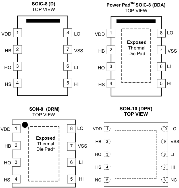
6 Pin Configuration and Functions

Pin Functions
| PIN | I/O | DESCRIPTION | ||
|---|---|---|---|---|
| NAME | D/DDA/DRM | DPR | ||
| VDD | 1 | 1 | P | Positive supply to the lower-gate driver. Decouple this pin to VSS (GND). Typical decoupling capacitor range is 0.22 µF to 4.7 µF (See (2)). |
| HB | 2 | 2 | P | High-side bootstrap supply. The bootstrap diode is on-chip but the external bootstrap capacitor is required. Connect positive side of the bootstrap capacitor to this pin. Typical range of HB bypass capacitor is 0.022 µF to 0.1 µF. The capacitor value is dependant on the gate charge of the high-side MOSFET and should also be selected based on speed and ripple criteria |
| HO | 3 | 3 | O | High-side output. Connect to the gate of the high-side power MOSFET. |
| HS | 4 | 4 | P | High-side source connection. Connect to source of high-side power MOSFET. Connect the negative side of bootstrap capacitor to this pin. |
| HI | 5 | 7 | I | High-side input.(3) |
| LI | 6 | 8 | I | Low-side input.(3) |
| VSS | 7 | 9 | G | Negative supply terminal for the device which is generally grounded. |
| LO | 8 | 10 | O | Low-side output. Connect to the gate of the low-side power MOSFET. |
| N/C | — | 5/6 | — | Not connected. |
| PowerPAD™(1) | Pad | Pad | G | Used on the DDA, DRM and DPR packages only. Electrically referenced to VSS (GND). Connect to a large thermal mass trace or GND plane to dramatically improve thermal performance. |
(1) The PowerPAD™ is not directly connected to any leads of the package. However it is electrically and thermally connected to the substrate which is the ground of the device.
(2) For cold temperature applications we recommend the upper capacitance range. Attention should also be made to PCB layout - see Layout.
(3) HI or LI input is assumed to connect to a low impedance source signal. The source output impedance is assumed less than 100 Ω. If the source impedance is greater than 100 Ω, add a bypassing capacitor, each, between HI and VSS and between LI and VSS. The added capacitor value depends on the noise levels presented on the pins, typically from 1 nF to 10 nF should be effective to eliminate the possible noise effect. When noise is present on two pins, HI or LI, the effect is to cause HO and LO malfunctions to have wrong logic outputs.