ZHCSLG6B June 2020 – April 2022 UCC27288
PRODUCTION DATA
- 1 特性
- 2 应用
- 3 说明
- 4 Revision History
- 5 Pin Configuration and Functions
- 6 Specifications
- 7 Detailed Description
- 8 Application and Implementation
- 9 Power Supply Recommendations
- 10Layout
- 11Device and Documentation Support
- 12Mechanical, Packaging, and Orderable Information
6.6 Switching Characteristics
VDD = VHB = 12 V, VHS = VSS = 0 V, No load on LO or HO, TJ = –40°C to +140°C, (unless otherwise noted)
| PARAMETER | TEST CONDITIONS | MIN | TYP | MAX | UNIT | |
|---|---|---|---|---|---|---|
| PROPAGATION DELAYS | ||||||
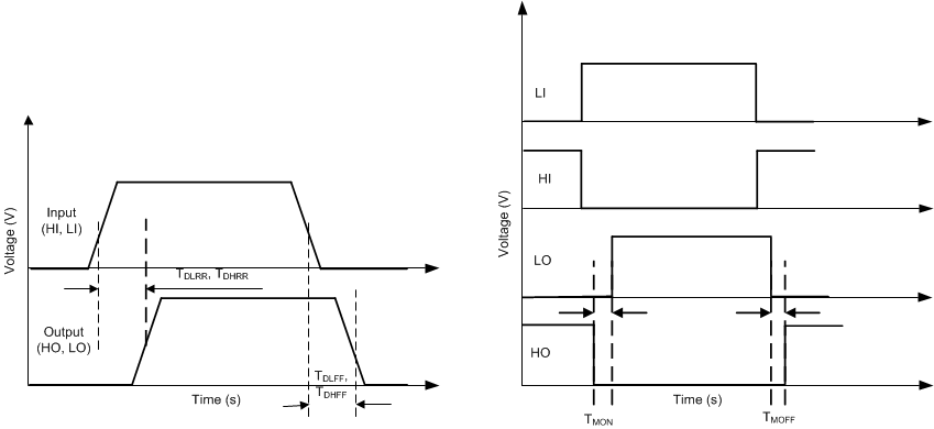
| tDLFF | VLI falling to VLO falling | See Figure 6-1 | 16 | 30 | ns | |
| tDHFF | VHI falling to VHO falling | See Figure 6-1 | 16 | 30 | ns | |
| tDLRR | VLI rising to VLO rising | See Figure 6-1 | 16 | 30 | ns | |
| tDHRR | VHI rising to VHO rising | See Figure 6-1 | 16 | 30 | ns | |
| DELAY MATCHING | ||||||
| tMON | From LO being ON to HO being OFF | See Figure 6-1 | 1 | 7 | ns | |
| tMOFF | From LO being OFF to HO being ON | See Figure 6-1 | 1 | 7 | ns | |
| OUTPUT RISE AND FALL TIME | ||||||
| tR | LO, HO rise time | CLOAD = 1800 pF, 10% to 90% | 12 | ns | ||
| tF | LO, HO fall time | CLOAD = 1800 pF, 90% to 10% | 10 | ns | ||
| tR | LO, HO (3 V to 9 V) rise time | CLOAD = 0.1 μF, 30% to 70% | 0.33 | 0.6 | μs | |
| tF | LO, HO (3 V to 9 V) fall time | CLOAD = 0.1 μF, 70% to 30% | 0.23 | 0.6 | μs | |
| MISCELLANEOUS | ||||||
| TPW,min | Minimum input pulse width that changes the output | 20 | ns | |||
 Figure 6-1 Timing Diagram