ZHCSQE6 October 2023 UCC27332-Q1
PRODUCTION DATA
- 1
- 1 特性
- 2 应用
- 3 说明
- 4 Revision History
- 5 Pin Configuration and Functions
- 6 Specifications
- 7 Detailed Description
- 8 Applications and Implementation
- 9 Device and Documentation Support
- 10Mechanical, Packaging, and Orderable Information
7.3.4 Output Stage
The output stage of the UCC27332-Q1 device is illustrated in Figure 7-2. The UCC27332-Q1 device features a P-Channel on the pull up structure, which delivers the highest peak source current when it is most needed during the Miller plateau region of the power switch turnon transition (when the power switch drain/collector voltage experiences dV/dt). This pull up architecture closely emulates the behavior of the popular industry driver devices UCC2732x. One characteristic of this pull up driver stage architecture is relatively consistent driver output rise and fall times over a wide VDD range.
 Figure 7-2 UCC27332-Q1 Gate Driver Output Stage
The ROH parameter (see Electrical Table) is a DC measurement and it is representative of the on-resistance of the P-Channel device on the pull up stage of the driver output. The pulldown structure is composed of a N-channel MOSFET only. The ROL is also a DC measurement, and it is representative of true impedance of the pulldown stage in the device.
The UCC27332-Q1 can deliver 9-A source, and up to 9-A sink at VDD = 14 V. Strong sink capability results in a very low pulldown impedance in the driver output stage which boosts immunity against the parasitic Miller turnon (high slew rate dV/dt turnon) effect that is seen in FET power switches.
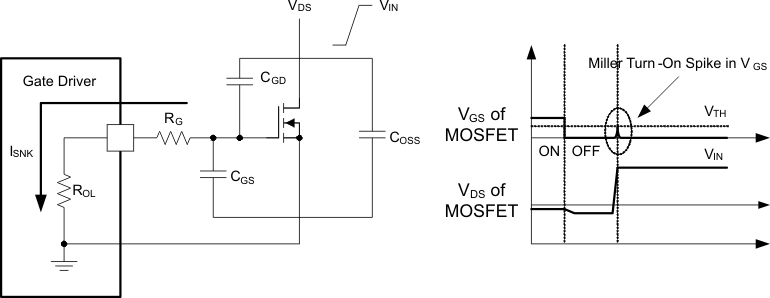
An example of a situation where Miller turnon is a concern is synchronous rectification (SR). In SR application, the dV/dt occurs on MOSFET drain when the MOSFET is already held in OFF state by the gate driver. The current charging the CGD Miller capacitance during this high dV/dt is shunted by the pulldown stage of the driver. If the pulldown impedance is not low enough then a voltage spike can result in the VGS of the MOSFET, which can result in spurious turnon. This phenomenon is illustrated in Figure 7-3.
 Figure 7-3 Low Pull-Down Impedance in UCC27332-Q1 (Output Stage Mitigates Miller Turnon Effect)
The driver output voltage swings between VDD and GND providing rail-to-rail operation because of the low dropout of the output stage. In most applications, the external Schottky diode clamps may be eliminated because the presence of the MOSFET body diodes offers low impedance to switching overshoots and undershoots. The output stage of the UCC27332-Q1 devices can handle significant transient reverse current. The two OUT pins of the device should be shorted on the application board. The application may use resistor and parallel diode-resistor combination at the gate of the MOSFET to program different rise (pullup current) time and fall (pulldown) time.