SLUS704C FEBRUARY 2007 – December 2014 UCC27423-EP , UCC27424-EP
PRODUCTION DATA.
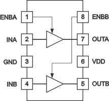
5 Pin Configuration and Functions
D or DGN Package
(Top View)

Pin Functions
| PIN | I/O | DESCRIPTION | |
|---|---|---|---|
| NAME | NO. | ||
| ENBA | 1 | I | Enable for driver A with logic-compatible threshold and hysteresis. The driver output can be enabled and disabled with this pin. It is pulled up internally to VDD with a 100-kΩ resistor for active-high operation. When the device is disabled, the output state is low, regardless of the input state. |
| ENBB | 8 | I | Enable for driver B with logic-compatible threshold and hysteresis. The driver output can be enabled and disabled with this pin. It is pulled up internally to VDD with a 100-kΩ resistor for active-high operation. The output state when the device is disabled is low, regardless of the input state. |
| GND | 3 | — | Common ground. This ground should be connected very closely to the source of the power MOSFET that the driver is driving. |
| INA | 2 | I | Input A. Input signal of the A driver, which has logic-compatible threshold and hysteresis. If not used, this input should be tied to either VDD or GND. Do not leave floating. |
| INB | 4 | I | Input B. Input signal of the A driver, which has logic-compatible threshold and hysteresis. If not used, this input should be tied to either VDD or GND. Do not leave floating. |
| OUTA | 7 | O | Driver output A. The output stage is capable of providing 4-A drive current to the gate of a power MOSFET. |
| OUTB | 5 | O | Driver output B. The output stage is capable of providing 4-A drive current to the gate of a power MOSFET. |
| VDD | 6 | I | Supply. Supply voltage and the power input connection for this device. |