ZHCSPQ0A may   2022  – july 2023 UCC27444-Q1

PRODUCTION DATA  

  1.   1
  2. 特性
  3. 应用
  4. 说明
  5. Revision History
  6. Pin Configuration and Functions
  7. Specifications
    1. 6.1 Absolute Maximum Ratings
    2. 6.2 ESD Ratings
    3. 6.3 Recommended Operating Conditions
    4. 6.4 Thermal Information
    5. 6.5 Electrical Characteristics
    6. 6.6 Switching Characteristics
    7. 6.7 Timing Diagrams
    8. 6.8 Typical Characteristics
  8. Detailed Description
    1. 7.1 Overview
    2. 7.2 Functional Block Diagram
    3. 7.3 Feature Description
      1. 7.3.1 Operating Supply Current
      2. 7.3.2 Input Stage
      3. 7.3.3 Enable Function
      4. 7.3.4 Output Stage
      5. 7.3.5 Low Propagation Delays and Tightly Matched Outputs
    4. 7.4 Device Functional Modes
  9. Application and Implementation
    1. 8.1 Application Information
    2. 8.2 Typical Application
      1. 8.2.1 Design Requirements
      2. 8.2.2 Detailed Design Procedure
        1. 8.2.2.1 VDD and Power On Reset
        2. 8.2.2.2 Drive Current and Power Dissipation
      3. 8.2.3 Application Curves
  10. Power Supply Recommendations
  11. 10Layout
    1. 10.1 Layout Guidelines
    2. 10.2 Layout Example
    3. 10.3 Thermal Considerations
  12. 11Device and Documentation Support
    1. 11.1 第三方米6体育平台手机版_好二三四免责声明
    2. 11.2 接收文档更新通知
    3. 11.3 支持资源
    4. 11.4 Trademarks
    5. 11.5 静电放电警告
    6. 11.6 术语表
  13. 12Mechanical, Packaging, and Orderable Information

封装选项

机械数据 (封装 | 引脚)
散热焊盘机械数据 (封装 | 引脚)
订购信息

Application Curves

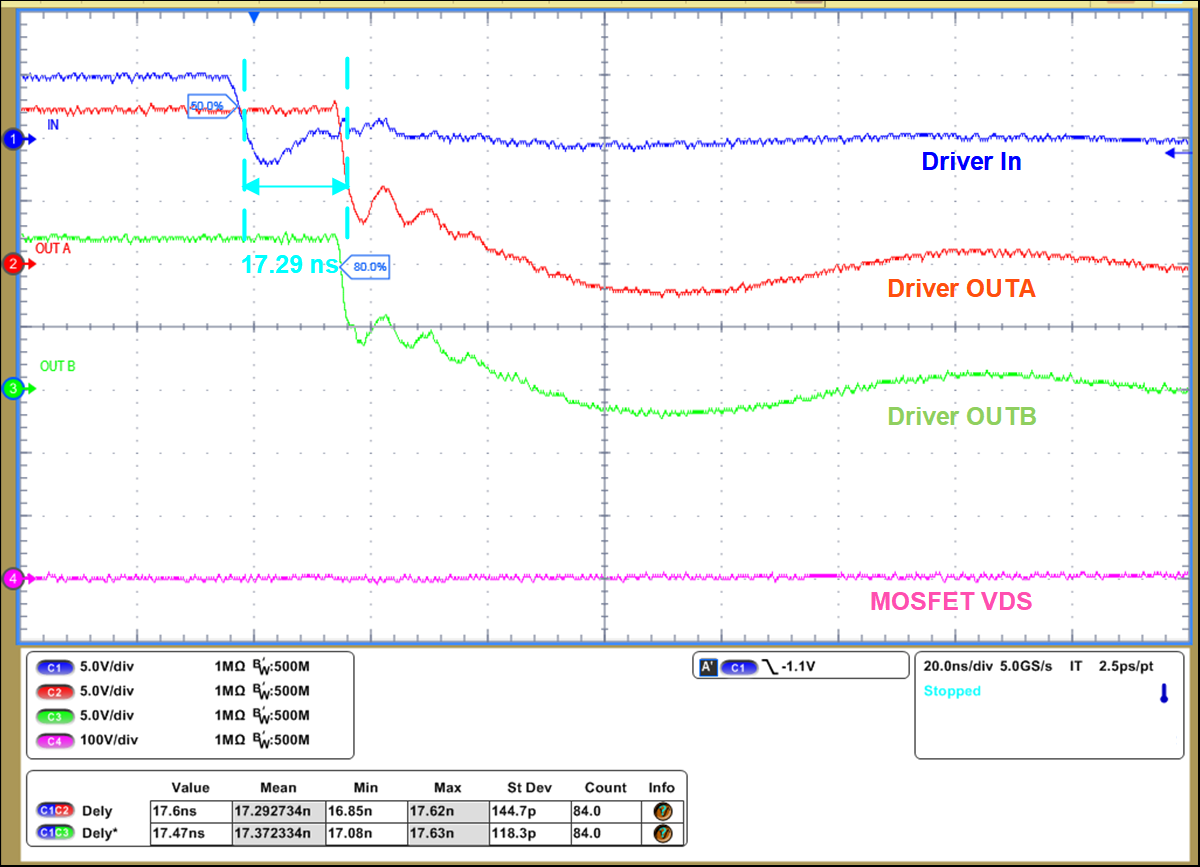
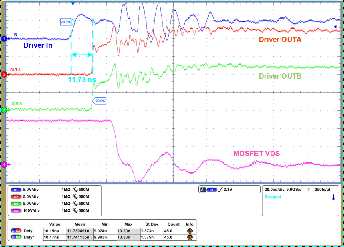
The figures below show the typical switching characteristics of the UCC27444-Q1 device used in high-voltage boost converter application. In this application, the UCC27444-Q1 is driving the IGBT switch that has a gate charge of
110nC.

GUID-20230718-SS0I-NZK3-SJWT-SP3HKRGM6G1X-low.svg Figure 8-3 UCC27444-Q1 Used to Drive IGBT in the Boost Converter
GUID-20230718-SS0I-SJ6L-LDFT-QNGXDH9GDGDM-low.png
Vin = 210 V, Vout= 235 V, Iout=1.1 A, Fsw=125 kHz, driver supply voltage=12 V, gate resistor= 0 Ω
Figure 8-4 Turn-On Propagation Delay Waveform
GUID-20230718-SS0I-NC1K-TNGN-MSK13G7SQSMP-low.png
Vin = 210 V, Vout= 235 V, Iout=1.1A, Fsw=125 kHz, driver supply voltage=12 V, gate resistor= 0 Ω
Figure 8-5 Turn-Off Propagation Delay Waveform