ZHCSPQ0A may   2022  – july 2023 UCC27444-Q1

PRODUCTION DATA  

  1.   1
  2. 特性
  3. 应用
  4. 说明
  5. Revision History
  6. Pin Configuration and Functions
  7. Specifications
    1. 6.1 Absolute Maximum Ratings
    2. 6.2 ESD Ratings
    3. 6.3 Recommended Operating Conditions
    4. 6.4 Thermal Information
    5. 6.5 Electrical Characteristics
    6. 6.6 Switching Characteristics
    7. 6.7 Timing Diagrams
    8. 6.8 Typical Characteristics
  8. Detailed Description
    1. 7.1 Overview
    2. 7.2 Functional Block Diagram
    3. 7.3 Feature Description
      1. 7.3.1 Operating Supply Current
      2. 7.3.2 Input Stage
      3. 7.3.3 Enable Function
      4. 7.3.4 Output Stage
      5. 7.3.5 Low Propagation Delays and Tightly Matched Outputs
    4. 7.4 Device Functional Modes
  9. Application and Implementation
    1. 8.1 Application Information
    2. 8.2 Typical Application
      1. 8.2.1 Design Requirements
      2. 8.2.2 Detailed Design Procedure
        1. 8.2.2.1 VDD and Power On Reset
        2. 8.2.2.2 Drive Current and Power Dissipation
      3. 8.2.3 Application Curves
  10. Power Supply Recommendations
  11. 10Layout
    1. 10.1 Layout Guidelines
    2. 10.2 Layout Example
    3. 10.3 Thermal Considerations
  12. 11Device and Documentation Support
    1. 11.1 第三方米6体育平台手机版_好二三四免责声明
    2. 11.2 接收文档更新通知
    3. 11.3 支持资源
    4. 11.4 Trademarks
    5. 11.5 静电放电警告
    6. 11.6 术语表
  13. 12Mechanical, Packaging, and Orderable Information

封装选项

机械数据 (封装 | 引脚)
散热焊盘机械数据 (封装 | 引脚)
订购信息

Typical Characteristics

Unless otherwise specified, VDD = 12 V, INx = 3.3 V, ENx = 3.3 V, TJ = 25°C, no load

GUID-20230707-SS0I-RZ5V-QDWH-0FMGCRFMMJFR-low.svg
Figure 6-3 Start-Up and Quiescent Current
GUID-20230703-SS0I-SLPM-3SGM-XWLTCRBCKCR6-low.svg
Figure 6-5 Static Supply Current (outputs in DC on or off condition)
GUID-20230701-SS0I-FDVM-FVT8-WB5RDJ3Q13WW-low.svg
Figure 6-7 Input Thresholds
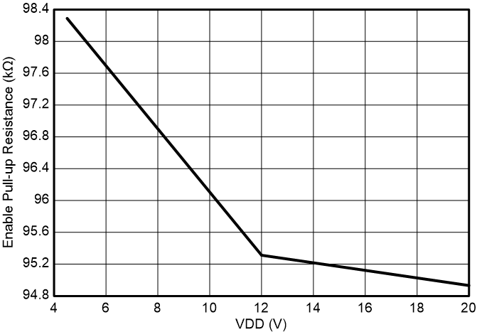
GUID-20230701-SS0I-J2SC-FCHS-HDQWHPBMRHKR-low.png
Figure 6-9 Enable Pullup Resistance
GUID-20230701-SS0I-BQVX-JXHD-6C8WRWCQP6GN-low.svg
Figure 6-11 Output Pulldown Resistance
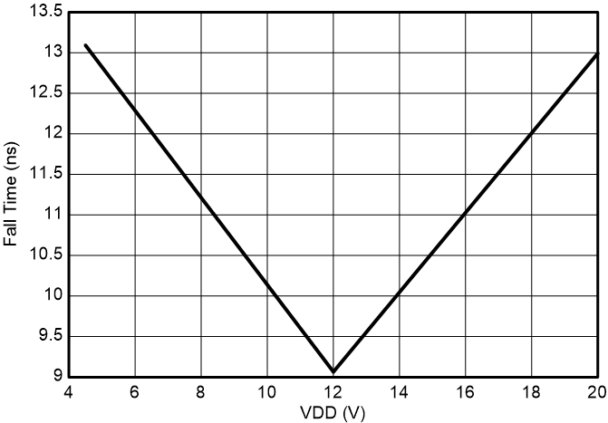
GUID-20230630-SS0I-9HFS-DJHZ-KFQFF9BJSMKQ-low.png
CLOAD = 1.8 nF
Figure 6-13 Output Fall Time vs VDD
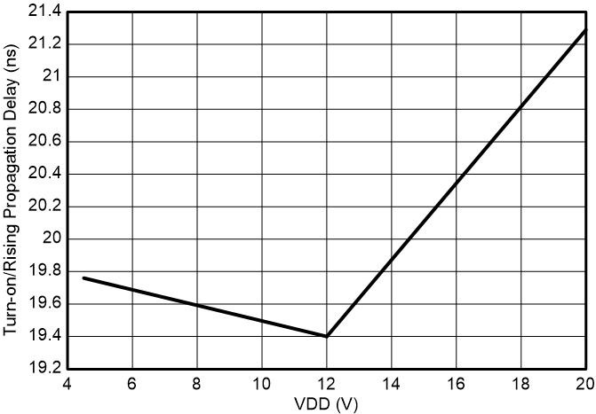
GUID-20230630-SS0I-0RZG-NQK1-PZP2BC2FCZPB-low.png
CLOAD = 1.8 nF
Figure 6-15 Input to Output Rising (turn-on) Propagation Delay vs VDD
GUID-20230630-SS0I-DBR1-ZCXG-S8FC0H292J6Q-low.svg
CLOAD = 1.8 nF
Figure 6-17 Input Propagation Delay vs Temperature
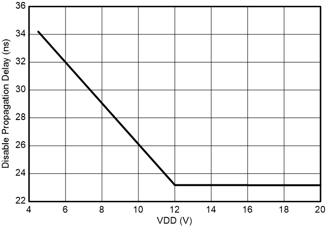
GUID-20230630-SS0I-DNXC-HZ3V-FVHHQDJHC9WD-low.png
CLOAD = 1.8 nF
Figure 6-19 Enable to Output Falling Propagation Delay
GUID-20230701-SS0I-0NNN-LSMK-CLC7FXP3NLQX-low.png
CLOAD = 1.8 nF
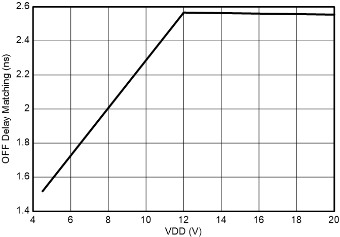
Figure 6-21 Turn-Off and Falling Delay Matching
GUID-20230628-SS0I-PPLD-BPHL-XL4VXKR92VGD-low.png
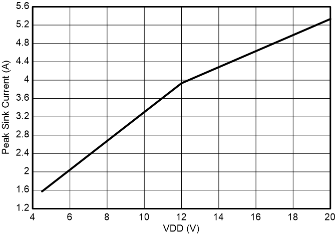
Figure 6-23 Peak Sink Current vs VDD
GUID-20230703-SS0I-J1HD-K41J-7BBKBS8CDVDG-low.png
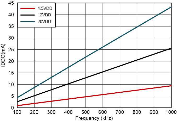
Figure 6-4 Operating Supply Current (both outputs switching)
GUID-20230703-SS0I-D6NR-H91C-PTJRHCF8RVBV-low.svg
Figure 6-6 Disable Current (EN = 0 V)
GUID-20230701-SS0I-55RX-XMH4-JQTKTC7TLKTX-low.png
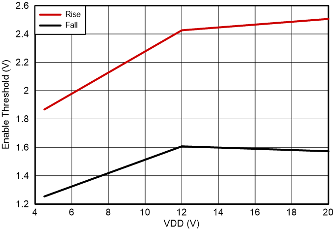
Figure 6-8 Enable Threshold
GUID-20230701-SS0I-6NB1-7SGK-MS1RSCS2ZP3F-low.svg
Figure 6-10 Output Pullup Resistance
GUID-20230630-SS0I-8WCC-WPNP-P3QQSZ7ZJN5C-low.png
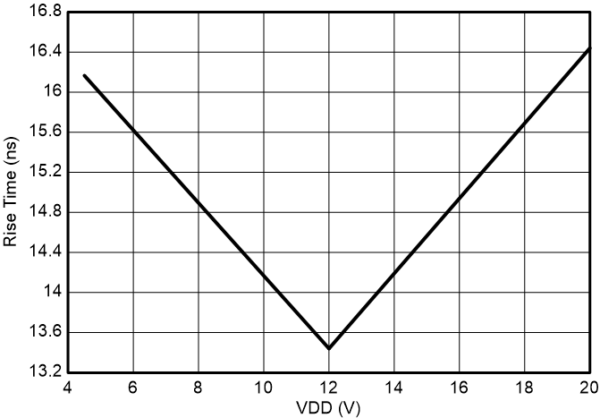
CLOAD = 1.8 nF
Figure 6-12 Output Rise Time vs VDD
GUID-20230630-SS0I-TLW6-NQ7W-S137BSWGNNHX-low.png
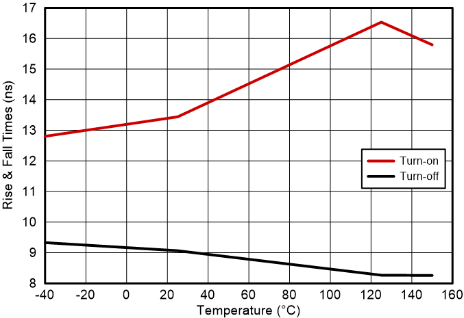
CLOAD = 1.8 nF
Figure 6-14 Output Rise and Fall Time vs Temperature
GUID-20230703-SS0I-SPC8-QMDT-XFK01VGBP564-low.svg
CLOAD = 1.8 nF
Figure 6-16 Input to Output Falling (turn-off) Propagation Delay vs VDD
GUID-20230630-SS0I-NHDS-XRPK-SNNKDB1VGB08-low.png
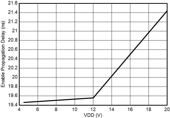
CLOAD = 1.8 nF
Figure 6-18 Enable to Output Rising Propagation Delay
GUID-20230701-SS0I-7W5G-RZC2-N9GFNSPGW2N2-low.svg
CLOAD = 1.8 nF
Figure 6-20 Turn-On/Rising Delay Matching
GUID-20230628-SS0I-NX5T-XDG1-NQPFM2XJRLXC-low.svg
Figure 6-22 Peak Source Current vs VDD