ZHCSHR6A March 2018 – January 2024 UCC27511A
PRODUCTION DATA
- 1
- 1 特性
- 2 应用
- 3 说明
- 4 Pin Configuration and Functions
- 5 Specifications
- 6 Detailed Description
- 7 Application and Implementation
- 8 Power Supply Recommendations
- 9 Layout
- 10Device and Documentation Support
- 11Revision History
- 12Mechanical, Packaging, and Orderable Information
6.3.5 Output Stage
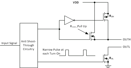
Figure 6-3 shows the output stage of the UCC27511A device. The UCC27511A device features a unique architecture on the output stage which delivers the highest peak-source current when the peak source current is most needed during the Miller plateau region of the power switch turnon transition (when the power-switch drain or collector voltage experiences dV/dt). The device output stage features a hybrid pullup structure using a parallel arrangement of N-channel and P-channel MOSFET devices. By turning on the N-channel MOSFET during a narrow instant when the output changes state from low to high, the gate-driver device is able to deliver a brief boost in the peak-sourcing current enabling fast turnon.
 Figure 6-3 UCC27511A Gate Driver Output Structure
The RO(H) parameter (see the Section 5.5 table) is a DC measurement and is representative of the on-resistance of the P-channel device only, because the N-Channel device is turned on only during output change of state from low to high. Thus the effective resistance of the hybrid pullup stage is much lower than what is represented by RO(H) parameter. The pulldown structure is composed of a N-channel MOSFET only. The RO(L) parameter (see the Section 5.5 table), which is also a DC measurement, is representative of true impedance of the pulldown stage in the device. In the UCC27511A device, the effective resistance of the hybrid pullup structure is approximately 2.7 × RO(L).
The UCC27511A device features a unique split output configuration where the gate-drive current is sourced through the OUTH pin and sunk through the OUTL pin. This unique pin arrangement allows users to apply independent turnon and turnoff resistors to the OUTH and OUTL pins respectively and easily control the turnon and turnoff switching dV/dt. This pin arrangement, along with the low pulldown impedance of the output driver stage, is especially useful in applications where a high C × dV/dt Miller turnon immunity is needed (such as with GaN power switches, SR MOSFETs and other applications) and the OUTL pin can be directly tied to the gate of the power device.
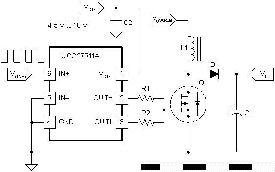
 Figure 6-4 Using
Non-Inverting Input (IN– Is Grounded To Enable Output)
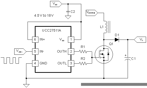
 Figure 6-5 Using
Inverting Input (IN+ Is Tied To VDD Enable Output)
Figure 6-5 Using
Inverting Input (IN+ Is Tied To VDD Enable Output)The UCC27511A device is capable of delivering 4-A source, 8-A sink (asymmetrical drive) at VDD equal to 12 V. Strong sink capability in asymmetrical drive results in a very-low pulldown impedance in the driver output stage which boosts immunity against parasitic, Miller turnon (C × dV/dt turnon) effect, especially where the low gate-charge MOSFETs or emerging wide band-gap GaN-power switches are used.
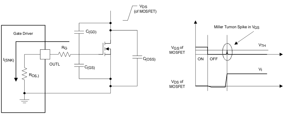
An example of a situation where the Miller turnon effect is a concern is synchronous rectification (SR). In an SR application, the dV/dt occurs on the MOSFET drain when the MOSFET is already held in off state by the gate driver. The current discharging the C(GD) Miller capacitance during this dV/dt is shunted by the pulldown stage of the driver. If the pulldown impedance is not low enough then a voltage spike can result in the VGS of the MOSFET, which can result in spurious turnon. This phenomenon is shown in Figure 6-6. The UCC27511A device offers a best-in-class, 0.375-Ω (typ) pulldown impedance boosting immunity against Miller turnon.
 Figure 6-6 Very-Low Pulldown Impedance in UCC27511A, 4-A and 8-A Asymmetrical Drive (Output Stage Mitigates Miller Turnon Effect)
The driver-output voltage swings between the VDD and GND pins which provides rail-to-rail operation as a result of the MOS-output stage which delivers very-low dropout. The presence of the MOSFET-body diodes also offers low impedance to switching overshoots and undershoots. In many cases, external Schottky diode clamps are eliminated. The outputs of these drivers are designed to withstand 500-mA reverse current without either damage to the device or logic malfunction.