ZHCS784D March 2012 – December 2014 UCC27516 , UCC27517
PRODUCTION DATA.
12 Layout
12.1 Layout Guidelines
Proper PCB layout is extremely important in a high-current fast-switching circuit to provide appropriate device operation and design robustness. The UCC27516 and UCC27517 gate driver incorporates short-propagation delays and powerful output stages capable of delivering large current peaks with very fast rise and fall times at the gate of the power switch to facilitate voltage transitions very quickly. At higher VDD voltages, the peak-current capability is even higher (4-A/4-A peak current is at VDD = 12 V). Very high di/dt causes unacceptable ringing if the trace lengths and impedances are not well controlled. The following circuit layout guidelines are strongly recommended when designing with these high-speed drivers.
- Locate the driver device as close as possible to the power device in order to minimize the length of high-current traces between the output pins and the gate of the power device.
- Locate the VDD bypass capacitors between VDD and GND as close as possible to the driver with minimal trace length to improve the noise filtering. These capacitors support high-peak current being drawn from VDD during turnon of power MOSFET. The use of low inductance SMD components such as chip resistors and chip capacitors is highly recommended.
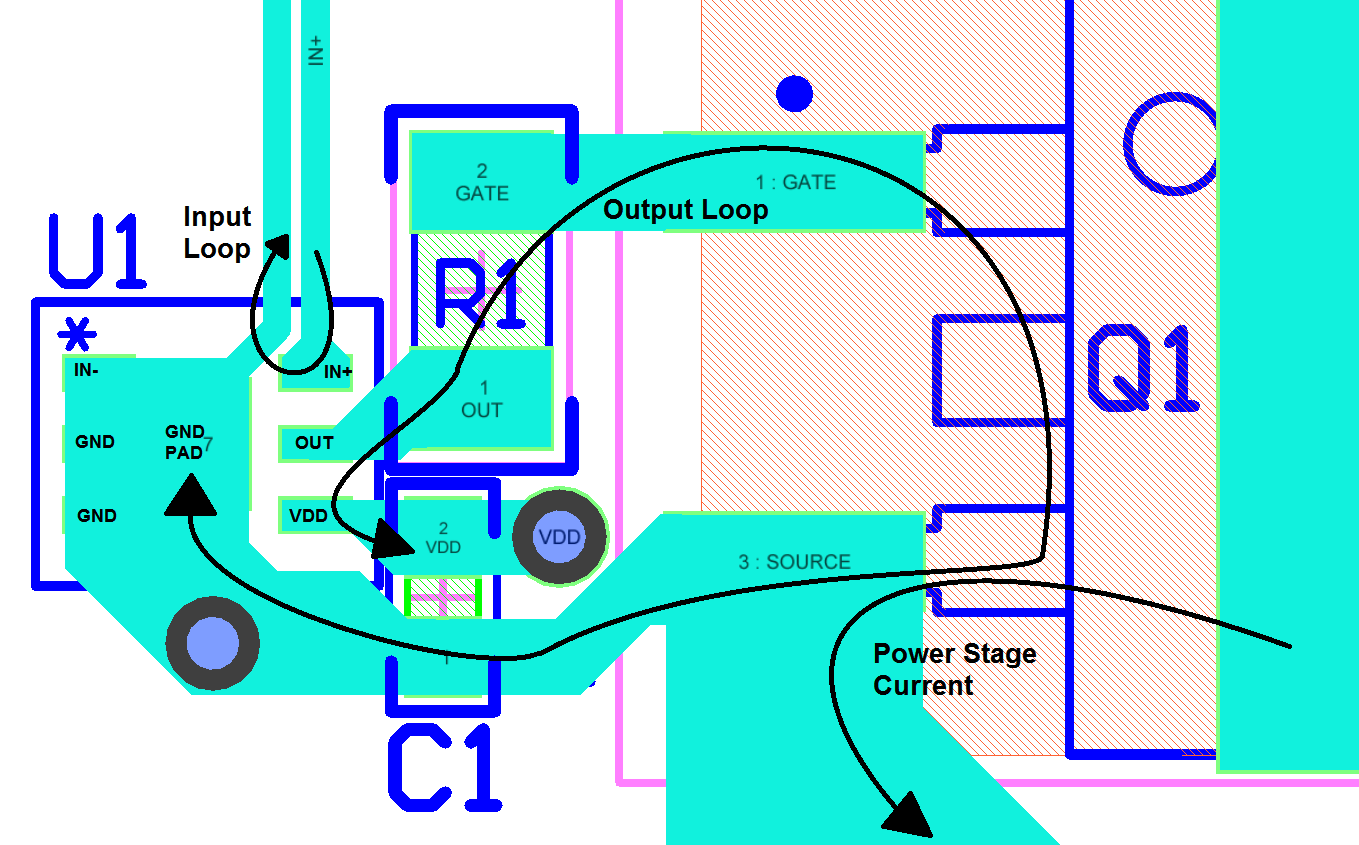
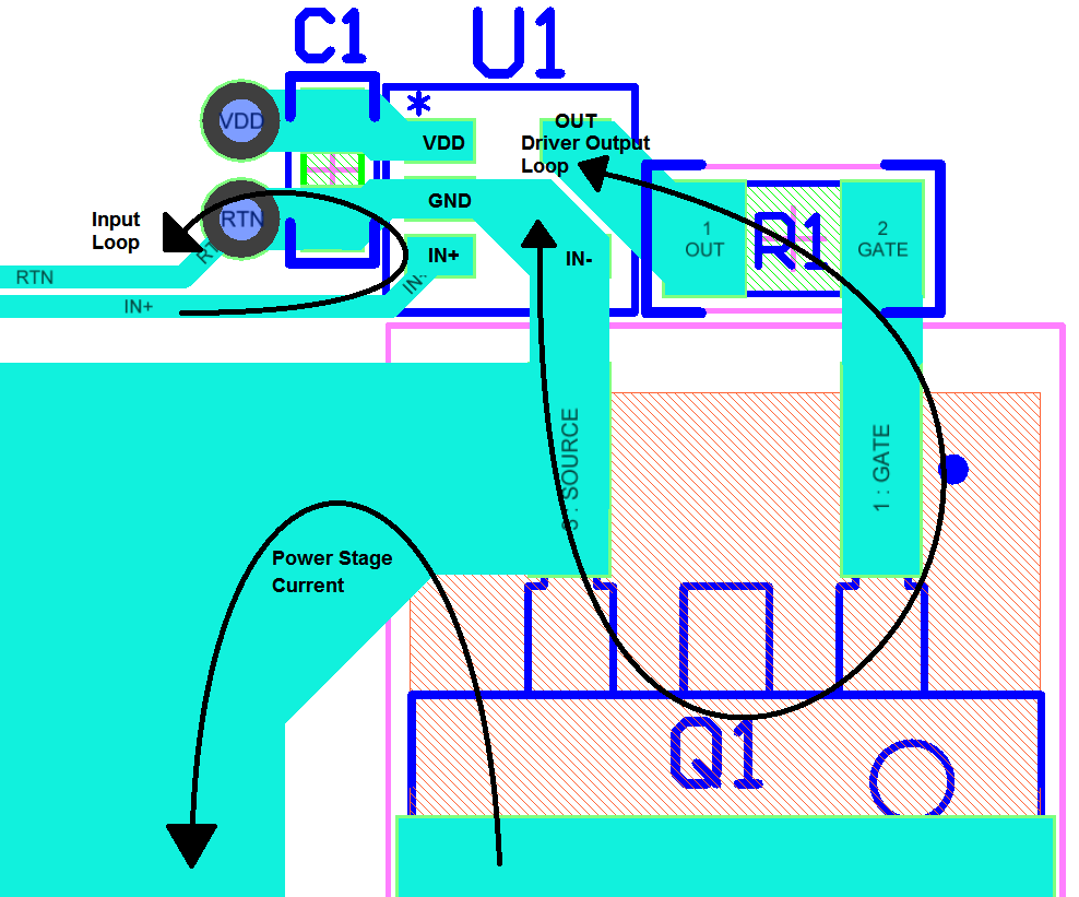
- The turnon and turnoff current-loop paths (driver device, power MOSFET and VDD bypass capacitor) should be minimized as much as possible in order to keep the stray inductance to a minimum. High dI/dt is established in these loops at two instances – during turnon and turnoff transients, which will induce significant voltage transients on the output pin of the driver device and gate of the power switch.
- Wherever possible parallel the source and return traces, taking advantage of flux cancellation.
- Separate power traces and signal traces, such as output and input signals.
- Star-point grounding is a good way to minimize noise coupling from one current loop to another. The GND of the driver should be connected to the other circuit nodes such as source of power switch or the ground of PWM controller at one, single point. The connected paths should be as short as possible to reduce inductance and be as wide as possible to reduce resistance.
- Use a ground plane to provide noise shielding. Fast rise and fall times at OUT may corrupt the input signals during transition. The ground plane must not be a conduction path for any current loop. Instead the ground plane must be connected to the star-point with one single trace to establish the ground potential. In addition to noise shielding, the ground plane can help in power dissipation as well.
- In noisy environments, tying the unused input pin of UCC27516 and UCC27517 to VDD (in case of IN+) or GND (in case of IN–) using short traces to ensure that the output is enabled and to prevent noise from causing malfunction in the output is necessary.
- The UCC27516 device offers two ground pins, pin 2 and pin 3. Shorting the two pins together using the PCB trace is extremely important. The shortest trace should be located as close as possible to the device.
12.2 Layout Example
 Figure 28. UCC27516DRS in Noninverting Configuration
 Figure 29. UCC27517DBV in Noninverting Configuration
12.3 Thermal Considerations
The useful range of a driver is greatly affected by the drive-power requirements of the load and the thermal characteristics of the package. For a gate driver to be useful over a particular temperature range the package must allow for the efficient removal of the heat produced while keeping the junction temperature within rated limits. The thermal metrics for the driver package is summarized in Thermal Information. For detailed information regarding the thermal information table, refer to the Application Note from Texas Instruments entitled IC Package Thermal Metrics (SPRA953).
The UCC27516 and UCC27517 devices are offered in SOT-23, 5-pin package (DBV) and 3 mm × 3 mm, WSON 6-pin package with exposed thermal pad (DRS), respectively. The Thermal Information table summarizes the thermal performance metrics related to the two packages. RθJA metric should be used for comparison of power dissipation between different packages. Under identical power dissipation conditions, the DRS package will maintain a lower die temperature than the DBV. The ψJT and ψJB metrics should be used when estimating the die temperature during actual application measurements.
The DRS is a better thermal package overall because of the exposed thermal pad and ability to sink heat to the PCB better than the DBV. The thermal pad in DRS package provides designers with an ability to create an excellent heat removal subsystem from the vicinity of the device, thus helping to maintain a lower junction temperature. This pad should be soldered to the copper on the printed circuit board directly underneath the device package. Then a printed circuit board designed with thermal lands and thermal vias completes a very efficient heat removal subsystem. In such a design, the heat is extracted from the semiconductor junction through the thermal pad, which is then efficiently conducted away from the location of the device on the PCB through the thermal network. This extraction helps to maintain a lower board temperature near the vicinity of the device leading to an overall lower device-junction temperature.
In comparison, for the DBV package, heat removal occurs primarily through the leads of the device and the PCB traces connected to the leads.
Note that the exposed pad in DRS package is not directly connected to any leads of the package. However, the DRS package is electrically and thermally connected to the substrate of the device which is the ground of the device. TI recommends to externally connect the exposed pads to GND in PCB layout for better EMI immunity.
12.4 Power Dissipation
Power dissipation of the gate driver has two portions as shown in Equation 1.

The DC portion of the power dissipation is PDC = IQ x VDD where IQ is the quiescent current for the driver. The quiescent current is the current consumed by the device to bias all internal circuits such as input stage, reference voltage, logic circuits, protections, and also any current associated with switching of internal devices when the driver output changes state (such as charging and discharging of parasitic capacitances, parasitic shoot-through etc). The UCC27516 and UCC27517 features very low quiescent currents (less than 1 mA, refer Figure 7) and contains internal logic to eliminate any shoot-through in the output-driver stage. Thus the effect of the PDC on the total power dissipation within the gate driver can be safely assumed to be negligible.
The power dissipated in the gate-driver package during switching (PSW) depends on the following factors:
- Gate charge required of the power device (usually a function of the drive voltage VG, which is very close to input bias supply voltage VDD due to low VOH drop-out).
- Switching frequency.
- Use of external-gate resistors.
When a driver device is tested with a discrete, capacitive load calculating the power that is required from the bias supply is fairly easy. The energy that must be transferred from the bias supply to charge the capacitor is given by Equation 2.

where
- CLOAD is load capacitor
- VDD is bias voltage feeding the driver
There is an equal amount of energy dissipated when the capacitor is charged. This leads to a total power loss given by Equation 3.

where
- ƒSW is the switching frequency
The switching load presented by a power MOSFET/IGBT is converted to an equivalent capacitance by examining the gate charge required to switch the device. This gate charge includes the effects of the input capacitance plus the added charge needed to swing the drain voltage of the power device as it switches between the ON and OFF states. Most manufacturers provide specifications of typical and maximum gate charge, in nC, to switch the device under specified conditions. Using the gate charge Qg, determine the power that must be dissipated when charging a capacitor. This is done by using the equation, QG = CLOAD x VDD, to provide Equation 4 for power:

This power PG is dissipated in the resistive elements of the circuit when the MOSFET/IGBT is being turned on or turned off. Half of the total power is dissipated when the load capacitor is charged during turnon, and the other half is dissipated when the load capacitor is discharged during turnoff. When no external gate resistor is employed between the driver and MOSFET/IGBT, this power is completely dissipated inside the driver package. With the use of external gate-drive resistors, the power dissipation is shared between the internal resistance of driver and external gate resistor in accordance to the ratio of the resistances (more power dissipated in the higher resistance component). Based on this simplified analysis, the driver power dissipation during switching is calculated in Equation 5.
