ZHCSBE0C August 2013 – August 2015 UCC27517A
PRODUCTION DATA.
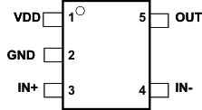
7 Pin Configuration and Functions
DBV Package
5-Pin SOT-23
Top View

Pin Functions
| PIN | I/O | DESCRIPTION | |
|---|---|---|---|
| NO. | NAME | ||
| 1 | VDD | I | Bias supply input. |
| 2 | GND | — | Ground. All signals reference to this pin. |
| 3 | IN+ | I | Non-inverting input. Apply PWM control signal to this pin when driver is desired to be operated in non-inverting configuration. When the driver is used in inverting configuration, connect IN+ to VDD in order to enable output, OUT held LOW if IN+ is unbiased or floating |
| 4 | IN- | I | Inverting input. Apply PWM control signal to this pin when driver is desired to be operated in inverting configuration. When the driver is used in non-inverting configuration, connect IN– to GND in order to enable output, OUT held LOW if IN– is unbiased or floating |
| 5 | OUT | O | Sourcing/Sinking current output of driver. |