ZHCS907A May 2012 – December 2014 UCC27518 , UCC27519
PRODUCTION DATA.
9 Detailed Description
9.1 Overview
The UCC2751x single-channel, high-speed, low-side gate-driver device is capable of effectively driving MOSFET and IGBT power switches. Using a design that inherently minimizes shoot-through current, the UCC2751x device is capable of sourcing and sinking high peak-current pulses into capacitive loads offering rail-to- rail drive capability and extremely small propagation delay of 13 ns (typical).
The UCC2751x device provides 4-A source, 4-A sink (symmetrical drive) peak-drive current capability. The device is designed to operate over a wide VDD range of 4.5 to 18 V, and a wide temperature range of -40°C to 140°C. Internal undervoltage lockout (UVLO) circuitry on the VDD pin holds the output low outside VDD operating range. The capability to operate at low voltage levels, such as below 5 V, along with best-in-class switching characteristics, is especially suited for driving emerging wide band-gap power-switching devices such as GaN power-semiconductor devices.
The UCC27518 device follows an inverting logic between the input and output, while the UCC27519 device follows noninverting logic. The input pins of the devices are based on what is known as CMOS input threshold logic. In CMOS input logic, the threshold voltage level is a function of the bias voltage on the VDD pin of the device. This offers the benefits of higher noise immunity due to the higher threshold voltage (compared to logic level input thresholds), as well as the ability to accept slow dV/dt input signals for manipulating the propagation delay between the PWM controller signal and the gate driver output. For system robustness, internal pull-up and pull-down resistors on the input pins ensure that outputs are held low when the input pins are in floating condition.
Table 2. UCC2751x Family of Features and Benefits
| FEATURE | BENEFIT |
|---|---|
| High Source/Sink Current Capability 4 A/8 A (Asymmetrical) – UCC27511/2 4 A/4 A (Symmetrical) – UCC27516/7 |
High current capability offers flexibility in employing UCC2751x family of devices to drive a variety of power switching devices at varying speeds |
| Best-in-class 13-ns (typ) Propagation delay | Extremely low pulse transmission distortion |
| Expanded VDD Operating range of 4.5 V to 18 V | Flexibility in system design Low VDD operation ensures compatibility with emerging wide band-gap power devices such as GaN |
| Expanded Operating Temperature range of -40 °C to 140 °C (See Electrical Characteristics table) |
|
| VDD UVLO Protection | Outputs are held low in UVLO condition, which ensures predictable, glitch-free operation at power-up and power-down |
| Outputs held low when input pins (INx) in floating condition | Safety feature, especially useful in passing abnormal condition tests during safety certification |
| Ability of input pins (and enable pin in UCC2751x) to handle voltage levels not restricted by VDD pin bias voltage | System simplification, especially related to auxiliary bias supply architecture |
| Split output structure in UCC27511 (OUTH, OUTL) | Allows independent optimization of turnon and turnoff speeds |
| Strong sink current (8 A) and low pull-down impedance (0.375 Ω) in UCC27511/2 | High immunity to C x dV/dt Miller turnon events |
| CMOS/TTL compatible input threshold logic with wide hysteresis in UCC27511/2/6/7 | Enhanced noise immunity, while retaining compatibility with microcontroller logic level input signals (3.3 V, 5 V) optimized for digital power |
| CMOS input threshold logic in UCC2751x (VIN_H – 70% VDD, VIN_L – 30% VDD) | Well suited for slow input voltage signals, with flexibility to program delay circuits (RCD) |
9.2 Functional Block Diagrams
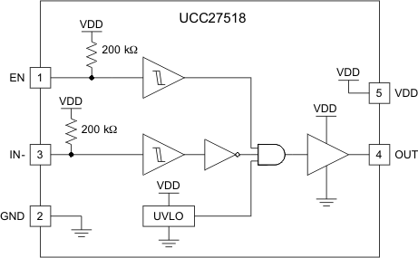 Figure 18. UCC27518 Functional Block Diagram
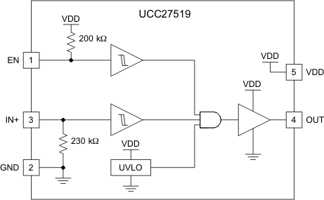 Figure 19. UCC27519 Functional Block Diagram
9.3 Feature Description
9.3.1 VDD and Undervoltage Lockout
The UCC2751x devices have internal Under Voltage LockOut (UVLO) protection feature on the VDD pin supply circuit blocks. Whenever the driver is in UVLO condition (i.e. when VDD voltage less than VON during power up and when VDD voltage is less than VOFF during power down), this circuit holds all outputs LOW, regardless of the status of the inputs. The UVLO is typically 4.2 V with 300-mV typical hysteresis. This hysteresis helps prevent chatter when low VDD supply voltages have noise from the power supply and also when there are droops in the VDD bias voltage when the system commences switching and there is a sudden increase in IDD. The capability to operate at low voltage levels such as below 5 V, along with best-in-class switching characteristics, is especially suited for driving emerging GaN wide bandgap power semiconductor devices.
For example, at power up, the UCC2751x driver output remains LOW until the VDD voltage reaches the UVLO threshold. The magnitude of the OUT signal rises with VDD until steady-state VDD is reached. In the noninverting device (PWM signal applied to IN+ pin) shown below, the output remains LOW until the UVLO threshold is reached, and then the output is in-phase with the input. In the inverting device (PWM signal applied to IN- pin) shown below the output remains LOW until the UVLO threshold is reached, and then the output is out-phase with the input.
Since the driver draws current from the VDD pin to bias all internal circuits, for the best high-speed circuit performance, two VDD bypass capacitors are recommended to prevent noise problems. The use of surface mount components is highly recommended. A 0.1-μF ceramic capacitor should be located as close as possible to the VDD to GND pins of the gate driver. In addition, a larger capacitor (such as 1 μF) with relatively low ESR should be connected in parallel and close proximity, in order to help deliver the high-current peaks required by the load. The parallel combination of capacitors should present a low impedance characteristic for the expected current levels and switching frequencies in the application.
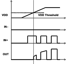 Figure 20. Power-Up (Noninverting Drive)
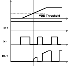 Figure 21. Power-Up (Inverting Drive)
9.3.2 Operating Supply Current
The UCC27518 and UCC27519 features very low quiescent IDD currents. The typical operating supply current in Under Voltage LockOut (UVLO) state and fully-on state (under static and switching conditions) are summarized in Figure 5, Figure 6 and Figure 7. The IDD current when the device is fully on and outputs are in a static state (DC high or DC low, refer Figure 7) represents lowest quiescent IDD current when all the internal logic circuits of the device are fully operational. The total supply current is the sum of the quiescent IDD current, the average IOUT current due to switching and finally any current related to pull-up resistors on the unused input pin. For example when the inverting input pin is pulled low additional current is drawn from VDD supply through the pull-up resistors (refer to Pin Configuration and Functions for the device Block Diagram). Knowing the operating frequency (fSW) and the MOSFET gate (QG) charge at the drive voltage being used, the average IOUT current can be calculated as product of QG and fSW.
A complete characterization of the IDD current as a function of switching frequency at different VDD bias voltages under 1.8-nF switching load is provided in Figure 15. The strikingly linear variation and close correlation with theoretical value of average IOUT indicates negligible shoot-through inside the gate-driver device attesting to its high-speed characteristics.
9.3.3 Input Stage
The input pins of UCC27518 and UCC27519 are based on CMOS input logic where the threshold voltage level is a function of the bias voltage applied on the VDD pin. Typically, the Input High Threshold (V_INH) is 55% VDD and Input Low Threshold (VIN_L) is 39% VDD. Hysteresis (typically 19% VDD) available on the input threshold offers noise immunity. With high VDD voltages resulting in wide hysteresis, slow dV/dt input signals are acceptable in the INx pins and RC circuits can be inserted between the input PWM signal and the INx pins of UCC2751x, to program a delay between the input signal and output transition.
9.3.4 Enable Function
The Enable pin is based on a noninverting configuration (active high operation). When EN pin is driven high the output is enabled and when EN pin is driven low the output is disabled. Unlike input pin, the enable pin threshold is based on a TTL/CMOS compatible input threshold logic that does not vary with the supply voltage. Typically, the Enable High Threshold (V_ENH) is 2.1 V and Enable Low Threshold (VEN_L) is 1.25 V. Thus the EN pin can be effectively controlled using logic signals from 3.3-V and 5-V microcontrollers. The EN pin is internally pulled up to VDD using pull-up resistor as a result of which the output of the device is enabled in the default state. Hence the EN pin can be left floating or Not Connected (N/C) for standard operation, when enable feature is not needed. Essentially, this allows the UCC27518/19 devices to be pin-to-pin compatible with TI’s previous generation drivers TPS2828/9 respectively, where pins #1 is N/C pin.
9.3.5 Output Stage
The UCC27518 and UCC27519 are capable of delivering 4-A source, 4-A sink (symmetrical drive) at VDD = 12 V. The output stage of the UCC27518 and UCC27519 devices are illustrated in Figure 22. The UCC27518 and UCC27519 devices features a unique architecture on the output stage which delivers the highest peak source current when it is most needed during the Miller plateau region of the power switch turnon transition (when the power switch drain/collector voltage experiences dV/dt). The device output stage features a hybrid pull-up structure using a parallel arrangement of N-Channel and P-Channel MOSFET devices. By turning on the N-Channel MOSFET during a narrow instant when the output changes state from low to high, the gate-driver device is able to deliver a brief boost in the peak-sourcing current enabling fast turn on.
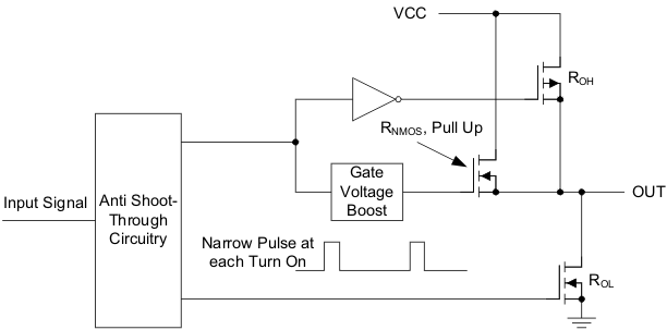 Figure 22. UCC2751x Gate Driver Output Structure
The ROH parameter (see Electrical Characteristics) is a DC measurement and it is representative of the on-resistance of the P-Channel device only, since the N-Channel device is turned on only during output change of state from low to high. Thus the effective resistance of the hybrid pull-up stage is much lower than what is represented by ROH parameter. The pull-down structure is composed of a N-Channel MOSFET only. The ROL parameter (see Electrical Characteristics), which is also a DC measurement, is representative of true impedance of the pull-down stage in the device. In UCC27518 and UCC27519, the effective resistance of the hybrid pull-up structure is approximately 1.4 x ROL.
The driver output voltage swings between VDD and GND providing rail-to-rail operation, thanks to the MOS output stage which delivers very low dropout. The presence of the MOSFET body diodes also offers low impedance to switching overshoots and undershoots. This means that in many cases, external Schottky diode clamps may be eliminated. The outputs of these drivers are designed to withstand 500-mA reverse current without either damage to the device or logic malfunction.
9.3.6 Low Propagation Delays
The UCC27518 and UCC27519 driver device features best-in-class input-to-output propagation delay of 17 ns (typ) at VDD = 12 V. This promises the lowest level of pulse transmission distortion available from industry standard gate driver devices for high-frequency switching applications. As seen in Figure 14, there is very little variation of the propagation delay with temperature and supply voltage as well, offering typically less than 20-ns propagation delays across the entire range of application conditions.