ZHCSBD7B August 2013 – October 2014 UCC27524A
PRODUCTION DATA.
- 1 特性
- 2 应用
- 3 说明
- 4 修订历史记录
- 5 说明(继续)
- 6 Pin Configuration and Functions
- 7 Specifications
- 8 Detailed Description
- 9 Applications and Implementation
- 10Power Supply Recommendations
- 11Layout
- 12器件和文档支持
- 13机械封装和可订购信息
封装选项
机械数据 (封装 | 引脚)
散热焊盘机械数据 (封装 | 引脚)
- DGN|8
订购信息
8 Detailed Description
8.1 Overview
The UCC27524A device represents Texas Instruments’ latest generation of dual-channel low-side high-speed gate-driver devices featuring a 5-A source and sink current capability, industry best-in-class switching characteristics, and a host of other features listed in Table 1 all of which combine to ensure efficient, robust and reliable operation in high-frequency switching power circuits.
Table 1. UCC27524A Features and Benefits
| FEATURE | BENEFIT |
|---|---|
| Best-in-class 13-ns (typ) propagation delay | Extremely low-pulse transmission distortion |
| 1-ns (typ) delay matching between channels | Ease of paralleling outputs for higher (2 times) current capability, ease of driving parallel-power switches |
| Expanded VDD Operating range of 4.5 to 18 V | Flexibility in system design |
| Expanded operating temperature range of –40 °C to +140 °C (See Electrical Characteristics table) |
|
| VDD UVLO Protection | Outputs are held Low in UVLO condition, which ensures predictable, glitch-free operation at power-up and power-down |
| Outputs held Low when input pins (INx) in floating condition | Safety feature, especially useful in passing abnormal condition tests during safety certification |
| Outputs enable when enable pins (ENx) in floating condition | Pin-to-pin compatibility with the UCC27324 device from Texas Instruments, in designs where Pin 1 and Pin 8 are in floating condition |
| CMOS/TTL compatible input and enable threshold with wide hysteresis | Enhanced noise immunity, while retaining compatibility with microcontroller logic-level input signals (3.3 V, 5 V) optimized for digital power |
| Ability of input and enable pins to handle voltage levels not restricted by VDD pin bias voltage | System simplification, especially related to auxiliary bias supply architecture |
| Ability to handle –5 VDC (max) at input pins | Increased robustness in noisy environments |
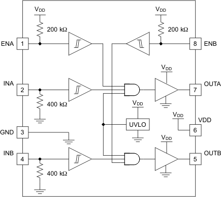
8.2 Functional Block Diagram
8.3 Feature Description
8.3.1 Operating Supply Current
The UCC27524A products feature very low quiescent IDD currents. The typical operating-supply current in UVLO state and fully-on state (under static and switching conditions) are summarized in Figure 3, Figure 4 and Figure 5. The IDD current when the device is fully on and outputs are in a static state (DC high or DC low, see Figure 4) represents lowest quiescent IDD current when all the internal logic circuits of the device are fully operational. The total supply current is the sum of the quiescent IDD current, the average IOUT current because of switching, and finally any current related to pullup resistors on the enable pins and inverting input pins. For example when the inverting input pins are pulled low additional current is drawn from the VDD supply through the pullup resistors (see though ). Knowing the operating frequency (fSW) and the MOSFET gate (QG) charge at the drive voltage being used, the average IOUT current can be calculated as product of QG and fSW.
A complete characterization of the IDD current as a function of switching frequency at different VDD bias voltages under 1.8-nF switching load in both channels is provided in Figure 15. The strikingly linear variation and close correlation with theoretical value of average IOUT indicates negligible shoot-through inside the gate-driver device attesting to its high-speed characteristics.
8.3.2 Input Stage
The input pins of UCC27524A gate-driver devices are based on a TTL and CMOS compatible input-threshold logic that is independent of the VDD supply voltage. With typically high threshold = 2.1 V and typically low threshold = 1.2 V, the logic level thresholds are conveniently driven with PWM control signals derived from 3.3-V and 5-V digital power-controller devices. Wider hysteresis (typ 0.9 V) offers enhanced noise immunity compared to traditional TTL logic implementations, where the hysteresis is typically less than 0.5 V. UCC27524A devices also feature tight control of the input pin threshold voltage levels which eases system design considerations and ensures stable operation across temperature (refer to Figure 7). The very low input capacitance on these pins reduces loading and increases switching speed.
The UCC27524A device features an important safety feature wherein, whenever any of the input pins is in a floating condition, the output of the respective channel is held in the low state. This is achieved using GND pulldown resistors on all the non-inverting input pins (INA, INB), as shown in the device block diagrams.
The input stage of each driver is driven by a signal with a short rise or fall time. This condition is satisfied in typical power supply applications, where the input signals are provided by a PWM controller or logic gates with fast transition times (<200 ns) with a slow changing input voltage, the output of the driver may switch repeatedly at a high frequency. While the wide hysteresis offered in UCC27524A definitely alleviates this concern over most other TTL input threshold devices, extra care is necessary in these implementations. If limiting the rise or fall times to the power device is the primary goal, then an external resistance is highly recommended between the output of the driver and the power device. This external resistor has the additional benefit of reducing part of the gate-charge related power dissipation in the gate driver device package and transferring it into the external resistor itself.
8.3.3 Enable Function
The enable function is an extremely beneficial feature in gate-driver devices especially for certain applications such as synchronous rectification where the driver outputs disable in light-load conditions to prevent negative current circulation and to improve light-load efficiency.
UCC27524A device is provided with independent enable pins ENx for exclusive control of each driver-channel operation. The enable pins are based on a non-inverting configuration (active-high operation). Thus when ENx pins are driven high the drivers are enabled and when ENx pins are driven low the drivers are disabled. Like the input pins, the enable pins are also based on a TTL and CMOS compatible input-threshold logic that is independent of the supply voltage and are effectively controlled using logic signals from 3.3-V and 5-V microcontrollers. The UCC27524A devices also feature tight control of the Enable-function threshold-voltage levels which eases system design considerations and ensures stable operation across temperature (refer to Figure 8). The ENx pins are internally pulled up to VDD using pullup resistors as a result of which the outputs of the device are enabled in the default state. Hence the ENx pins are left floating or Not Connected (N/C) for standard operation, where the enable feature is not needed. Essentially, this floating allows the UCC27524A device to be pin-to-pin compatible with TI’s previous generation of drivers (UCC27323, UCC27324, and UCC27325 respectively), where Pin 1 and Pin 8 are N/C pins. If the channel A and Channel B inputs and outputs are connected in parallel to increase the driver current capacity, ENA and ENB are connected and driven together.
8.3.4 Output Stage
The UCC27524A device output stage features a unique architecture on the pullup structure which delivers the highest peak-source current when it is most needed during the Miller plateau region of the power-switch turnon transition (when the power switch drain or collector voltage experiences dV/dt). The output stage pullup structure features a P-Channel MOSFET and an additional N-Channel MOSFET in parallel. The function of the N-Channel MOSFET is to provide a brief boost in the peak sourcing current enabling fast turnon. This is accomplished by briefly turning-on the N-Channel MOSFET during a narrow instant when the output is changing state from Low to High.
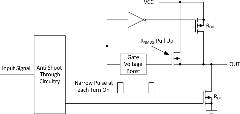 Figure 20. UCC27524A Gate Driver Output Structure
The ROH parameter (see Electrical Characteristics) is a DC measurement and it is representative of the on-resistance of the P-Channel device only. This is because the N-Channel device is held in the off state in DC condition and is turned-on only for a narrow instant when output changes state from low to high. Note that effective resistance of the UCC27524A pullup stage during the turnon instant is much lower than what is represented by ROH parameter.
The pulldown structure in the UCC27524A device is simply composed of a N-Channel MOSFET. The ROL parameter (see Electrical Characteristics), which is also a DC measurement, is representative of the impedance of the pulldown stage in the device. In the UCC27524A device, the effective resistance of the hybrid pullup structure during turnon is estimated to be approximately 1.5 × ROL, estimated based on design considerations.
Each output stage in the UCC27524A device is capable of supplying 5-A peak source and 5-A peak sink current pulses. The output voltage swings between VDD and GND providing rail-to-rail operation, thanks to the MOS-output stage which delivers very low drop-out. The presence of the MOSFET-body diodes also offers low impedance to switching overshoots and undershoots which means that in many cases, external Schottky-diode clamps may be eliminated. The outputs of these drivers are designed to withstand 500-mA reverse current without either damage to the device or logic malfunction.
The UCC27524A device is particularly suited for dual-polarity, symmetrical drive-gate transformer applications where the primary winding of transformer driven by OUTA and OUTB, with inputs INA and INB being driven complementary to each other. This situation is because of the extremely low drop-out offered by the MOS output stage of these devices, both during high (VOH) and low (VOL) states along with the low impedance of the driver output stage, all of which allow alleviate concerns regarding transformer demagnetization and flux imbalance. The low propagation delays also ensure accurate reset for high-frequency applications.
For applications that have zero voltage switching during power MOSFET turnon or turnoff interval, the driver supplies high-peak current for fast switching even though the miller plateau is not present. This situation often occurs in synchronous rectifier applications because the body diode is generally conducting before power MOSFET is switched on.
8.3.5 Low Propagation Delays And Tightly Matched Outputs
The UCC27524A driver device features a best in class, 13-ns (typical) propagation delay between input and output which goes to offer the lowest level of pulse-transmission distortion available in the industry for high frequency switching applications. For example in synchronous rectifier applications, the SR MOSFETs are driven with very low distortion when a single driver device is used to drive both the SR MOSFETs. Further, the driver devices also feature an extremely accurate, 1-ns (typical) matched internal-propagation delays between the two channels which is beneficial for applications requiring dual gate drives with critical timing. For example in a PFC application, a pair of paralleled MOSFETs can be driven independently using each output channel, which the inputs of both channels are driven by a common control signal from the PFC controller device. In this case the 1-ns delay matching ensures that the paralleled MOSFETs are driven in a simultaneous fashion with the minimum of turnon delay difference. Yet another benefit of the tight matching between the two channels is that the two channels are connected together to effectively increase current drive capability, for example A and B channels may be combined into a single driver by connecting the INA and INB inputs together and the OUTA and OUTB outputs together. Then, a single signal controls the paralleled combination.
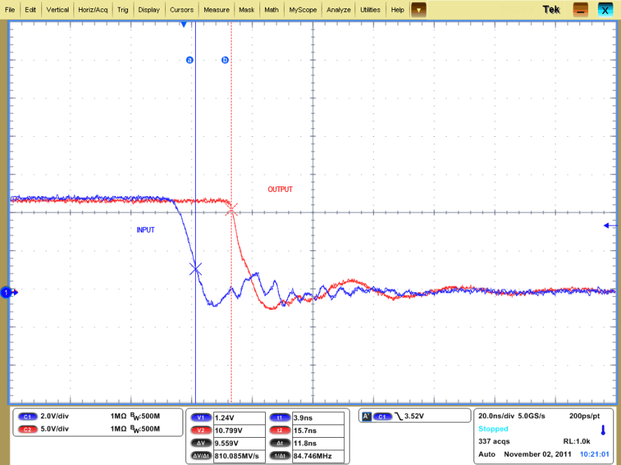
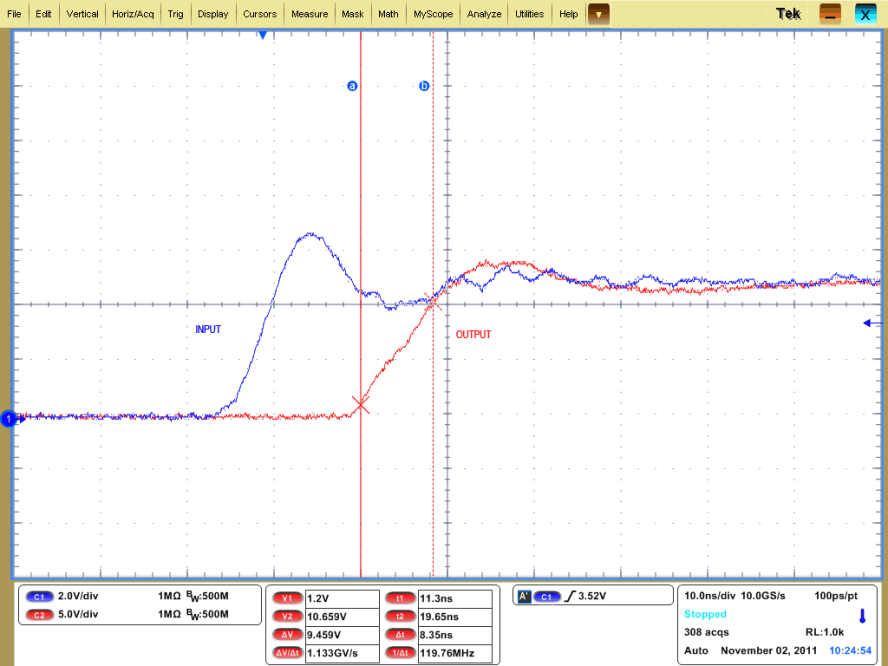
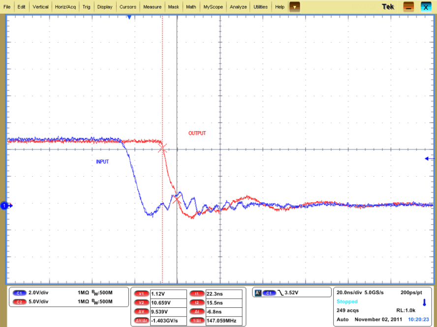
Caution must be exercised when directly connecting OUTA and OUTB pins together because there is the possibility that any delay between the two channels during turnon or turnoff may result in shoot-through current conduction as shown in Figure 21. While the two channels are inherently very well matched (4-ns Max propagation delay), note that there may be differences in the input threshold voltage level between the two channels which causes the delay between the two outputs especially when slow dV/dt input signals are employed. The following guidelines are recommended whenever the two driver channels are paralleled using direct connections between OUTA and OUTB along with INA and INB:
- Use very fast dV/dt input signals (20 V/µs or greater) on INA and INB pins to minimize impact of differences in input thresholds causing delays between the channels.
- INA and INB connections must be made as close to the device pins as possible.
Wherever possible, a safe practice would be to add an option in the design to have gate resistors in series with OUTA and OUTB. This allows the option to use 0-Ω resistors for paralleling outputs directly or to add appropriate series resistances to limit shoot-through current, should it become necessary.
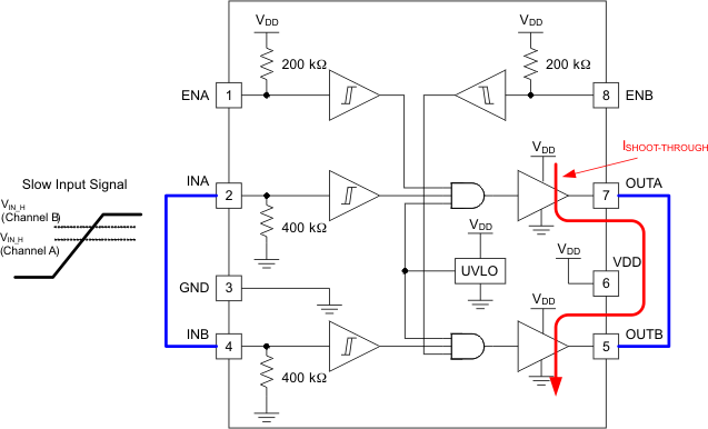 Figure 21. Slow Input Signal Can Cause Shoot-Through Between Channels During Paralleling
 (Recommended DV/DT is 20 V/Μs or Higher)
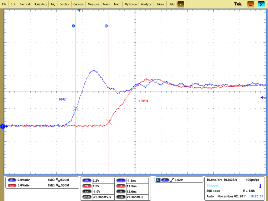
(CL = 1.8 nF, VDD = 12 V)
(CL = 1.8 nF, VDD = 12 V)
(CL = 1.8 nF, VDD = 12 V)
(CL = 1.8 nF, VDD = 12 V)