ZHCSGK8 April 2017 UCC27524A1-Q1
PRODUCTION DATA.
9 Application and Implementation
NOTE
Information in the following applications sections is not part of the TI component specification, and TI does not warrant its accuracy or completeness. TI’s customers are responsible for determining suitability of components for their purposes. Customers should validate and test their design implementation to confirm system functionality.
9.1 Application Information
High-current gate-driver devices are required in switching power applications for a variety of reasons. In order to effect the fast switching of power devices and reduce associated switching-power losses, a powerful gate-driver device employs between the PWM output of control devices and the gates of the power semiconductor devices. Further, gate-driver devices are indispensable when it is not feasible for the PWM controller device to directly drive the gates of the switching devices. With the advent of digital power, this situation is often encountered because the PWM signal from the digital controller is often a 3.3-V logic signal which is not capable of effectively turning on a power switch. A level-shifting circuitry is required to boost the 3.3-V signal to the gate-drive voltage (such as 12 V) in order to fully turn on the power device and minimize conduction losses. Traditional buffer-drive circuits based on NPN/PNP bipolar transistors in a totem-pole arrangement, as emitter-follower configurations, prove inadequate with digital power because the traditional buffer-drive circuits lack level-shifting capability. Gate-driver devices effectively combine both the level-shifting and buffer-drive functions. Gate-driver devices also find other needs such as minimizing the effect of high-frequency switching noise by locating the high-current driver physically close to the power switch, driving gate-drive transformers and controlling floating power-device gates, reducing power dissipation and thermal stress in controller devices by moving gate-charge power losses into the controller. Finally, emerging wide band-gap power-device technologies such as GaN based switches, which are capable of supporting very high switching frequency operation, are driving special requirements in terms of gate-drive capability. These requirements include operation at low VDD voltages (5 V or lower), low propagation delays, tight delay matching and availability in compact, low-inductance packages with good thermal capability. In summary, gate-driver devices are an extremely important component in switching power combining benefits of high-performance, low-cost, component-count, board-space reduction, and simplified system design.
9.2 Typical Application
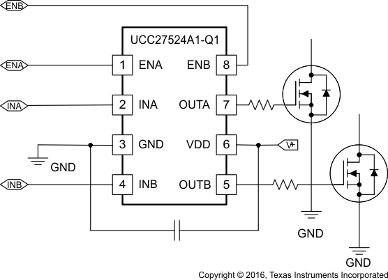
 Figure 26. UCC27524A1-Q1 Typical Application Diagram
9.2.1 Design Requirements
When selecting the proper gate driver device for an end application, some desiring considerations must be evaluated first in order to make the most appropriate selection. Among these considerations are VDD, UVLO, Drive current and power dissipation.
9.2.2 Detailed Design Procedure
9.2.2.1 VDD and Undervoltage Lockout
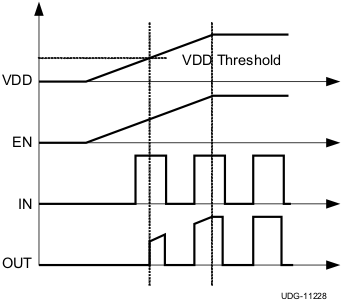
The UCC27524A1-Q1 device has an internal undervoltage-lockout (UVLO) protection feature on the VDD pin supply circuit blocks. When VDD is rising and the level is still below UVLO threshold, this circuit holds the output low, regardless of the status of the inputs. The UVLO is typically 4.25 V with 350-mV typical hysteresis. This hysteresis prevents chatter when low VDD supply voltages have noise from the power supply and also when there are droops in the VDD bias voltage when the system commences switching and there is a sudden increase in IDD. The capability to operate at low voltage levels such as below 5 V, along with best in class switching characteristics, is especially suited for driving emerging GaN power semiconductor devices.
For example, at power up, the UCC27524A1-Q1 driver-device output remains low until the VDD voltage reaches the UVLO threshold if enable pin is active or floating. The magnitude of the OUT signal rises with VDD until steady-state VDD is reached. The operation in Figure 27 shows that the output remains low until the UVLO threshold is reached, and then the output is in-phase with the input.
Because the device draws current from the VDD pin to bias all internal circuits, for the best high-speed circuit performance, two VDD bypass capacitors are recommended to prevent noise problems. The use of surface mount components is highly recommended. A 0.1-μF ceramic capacitor must be located as close as possible to the VDD to GND pins of the gate-driver device. In addition, a larger capacitor (such as 1-μF) with relatively low ESR must be connected in parallel and close proximity, in order to help deliver the high-current peaks required by the load. The parallel combination of capacitors presents a low impedance characteristic for the expected current levels and switching frequencies in the application.
 Figure 27. Power-Up Non-Inverting Driver
9.2.2.2 Drive Current and Power Dissipation
The UCC27524A1-Q1 driver is capable of delivering 5-A of current to a MOSFET gate for a period of several-hundred nanoseconds at VDD = 12 V. High peak current is required to turn the device ON quickly. Then, to turn the device OFF, the driver is required to sink a similar amount of current to ground which repeats at the operating frequency of the power device. The power dissipated in the gate driver device package depends on the following factors:
- Gate charge required of the power MOSFET (usually a function of the drive voltage VGS, which is very close to input bias supply voltage VDD due to low VOH drop-out)
- Switching frequency
- Use of external gate resistors
Because UCC27524A1-Q1 features very low quiescent currents and internal logic to eliminate any shoot-through in the output driver stage, their effect on the power dissipation within the gate driver can be safely assumed to be negligible.
When a driver device is tested with a discrete, capacitive load calculating the power that is required from the bias supply is fairly simple. The energy that must be transferred from the bias supply to charge the capacitor is given by Equation 1.

where
- CLOAD is the load capacitor
- VDD2 is the bias voltage feeding the driver
There is an equal amount of energy dissipated when the capacitor is charged. This leads to a total power loss given by Equation 2.

where
- fSW is the switching frequency
With VDD = 12 V, CLOAD = 10 nF and fSW = 300 kHz the power loss is calculated with Equation 3.

The switching load presented by a power MOSFET is converted to an equivalent capacitance by examining the gate charge required to switch the device. This gate charge includes the effects of the input capacitance plus the added charge needed to swing the drain voltage of the power device as it switches between the ON and OFF states. Most manufacturers provide specifications that provide the typical and maximum gate charge, in nC, to switch the device under specified conditions. Using the gate charge Qg, the power that must be dissipated when charging a capacitor is determined which by using the equivalence Qg = CLOADVDD to provide Equation 4 for power:

Assuming that the UCC27524A1-Q1 device is driving power MOSFET with 60 nC of gate charge (Qg = 60 nC at VDD = 12 V) on each output, the gate charge related power loss is calculated with Equation 5.

This power PG is dissipated in the resistive elements of the circuit when the MOSFET turns on or turns off. Half of the total power is dissipated when the load capacitor is charged during turnon, and the other half is dissipated when the load capacitor is discharged during turnoff. When no external gate resistor is employed between the driver and MOSFET/IGBT, this power is completely dissipated inside the driver package. With the use of external gate drive resistors, the power dissipation is shared between the internal resistance of driver and external gate resistor in accordance to the ratio of the resistances (more power dissipated in the higher resistance component). Based on this simplified analysis, the driver power dissipation during switching is calculated as follows (see Equation 6):

where
- ROFF = ROL
- RON (effective resistance of pullup structure) = 1.5 x ROL
In addition to the above gate-charge related power dissipation, additional dissipation in the driver is related to the power associated with the quiescent bias current consumed by the device to bias all internal circuits such as input stage (with pullup and pulldown resistors), enable, and UVLO sections. As shown in Figure 4, the quiescent current is less than 0.6 mA even in the highest case. The quiescent power dissipation is calculated easily with Equation 7.

Assuming , IDD = 6 mA, the power loss is:

Clearly, this power loss is insignificant compared to gate charge related power dissipation calculated earlier.
With a 12-V supply, the bias current is estimated as follows, with an additional 0.6-mA overhead for the quiescent consumption:


