ZHCSAO3E June 2013 – December 2014 UCC27527 , UCC27528
PRODUCTION DATA.
9 Application and Implementation
NOTE
Information in the following applications sections is not part of the TI component specification, and TI does not warrant its accuracy or completeness. TI’s customers are responsible for determining suitability of components for their purposes. Customers should validate and test their design implementation to confirm system functionality.
9.1 Application Information
High-current gate-driver devices are required in switching power applications for a variety of reasons. In order to effect fast switching of power devices and reduce associated switching power losses, a powerful gate driver device can be employed between the PWM output of control devices and the gates of the power semiconductor devices. Further, gate driver devices are indispensable when sometimes it is just not feasible to have the PWM controller device directly drive the gates of the switching devices. With advent of digital power, this situation will be often encountered since the PWM signal from the digital controller is often a 3.3-V logic signal which is not capable of effectively turning on a power switch. A level shifting circuitry is needed to boost the 3.3-V signal to the gate-drive voltage (such as 12 V) in order to fully turn on the power device and minimize conduction losses. Traditional buffer drive circuits based on NPN/PNP bipolar transistors in totem-pole arrangement, being emitter follower configurations, prove inadequate with digital power since they lack level-shifting capability. Gate driver devices effectively combine both the level-shifting and buffer drive functions. Gate driver devices also find other needs such as minimizing the effect of high-frequency switching noise by locating the high-current driver physically close to the power switch, driving gate drive transformers and controlling floating power device gates, reducing power dissipation and thermal stress in controller devices by moving gate charge power losses into itself. In summary Gate-driver devices are an extremely important component in switching power combining benefits of high performance, low cost, component count, board-space reduction and simplified system design.
9.2 Typical Application
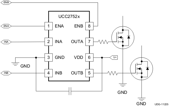 Figure 29. UCC2752x Typical Application Diagram (X = 8)
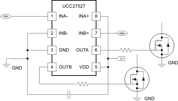 Figure 30. UCC27527 Typical Application Diagram
 Channel A in Inverting and Channel B in Non-Inverting Configuration,
(Enable Function Not Used)
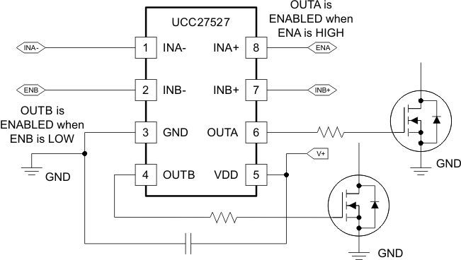 Figure 31. UCC27527 Typical Application Diagram
Channel A In Inverting And Channel B In Non-Inverting Configuration,
(Enable Function Implemented)
9.2.1 Design Requirements
When selecting the proper gate driver device for an end application, some design considerations must be evaluated first in order to make the most appropriate selection. Among these considerations are Input-to-Output Logic, Enable and Disable function, VDD, Propagation delay, and power dissipation.
9.2.2 Detailed Design Procedure
9.2.2.1 Input-to-Output Logic
The design should specify which type of input-to-output configuration should be used. UCC27528 can only provide dual non-inverting input-to-output with enable control. If turning on the power MOSFET or IGBT when the input signal is in high state is preferred, then the non-inverting configuration must be selected. If turning off the power MOSFET or IGBT when the input signal is in high state is preferred, the inverting configuration must be chosen. UCC27527 has dual configuration channel. Each Channel of UCC27527 device can be configured in either an inverting or non-inverting input-to-output configuration using the INx– or INx+ pins respectively like in Figure 30 and Figure 31. To configure the channel for use in inverting mode, tie the INx+ pin to VDD and apply the input signal to the INx– pin. For the non-inverting configuration, tie the INx– pin to GND and apply the input signal to the INx+ pin.
9.2.2.2 Enable and Disable Function
Certain applications demand independent control of the output state of the driver. UCC278525 device offers two independent enable pins ENx for exclusive control of each driver channels as listed in Table 2. The UCC27527 device does not feature dedicated enable pins. However, as mentioned earlier, an enable/disable function can be easily implemented in UCC27527 using the unused input pin. When INx+ is pulled-down to GND or INx- is pulled-down to VDD, the output is disabled. Thus INx+ pin can be used like an enable pin that is based on active high logic, while INx- can be used like an enable pin that is based on active low logic. It is important to note that while the ENA, ENB pins in the UCC27528 are allowed to be in floating condition during standard operation and the outputs will be enabled, the INx+, INx- pins in UCC27527 are not allowed to be floating since this will disable the outputs.
9.2.2.3 VDD Bias Supply Voltage
The bias supply voltage to be applied to the VDD pin of the device should never exceed the values listed in the Recommended Operating Conditions table. However, different power switches demand different voltage levels to be applied at the gate terminals for effective turnon and turnoff. With certain power switches, a positive gate voltage may be required for turnon and a negative gate voltage may be required for turnoff, in which case the VDD bias supply equals the voltage differential. With a wide operating range from 4.5 V to 18 V, the UCC2752X device can be used to drive a variety of power switches, such as Si MOSFETs (for example, VGS = 4.5 V, 10V, 12 V), IGBTs (VGE = 15 V, 18 V), and wide-bandgap power semiconductors (such as GaN, certain types of which allow no higher than 6 V to be applied to the gate pins).
9.2.2.4 Propagation Delay
The acceptable propagation delay from the gate driver is dependent on the switching frequency at which it is used and the acceptable level of pulse distortion to the system. The UCC2752X device features fast 17-ns (typical) propagation delays which ensures very little pulse distortion and allows operation at very high-frequencies. See the Switching Characteristics table for the propagation and switching characteristics of the UCC2752X device. For certain application which needed programmable propagation delay, The UCC2752X device can accept slow dv/dt input signals which allows designers to use RCD circuits on the input pin to program propagation as in Figure 26.
9.2.2.5 Drive Current and Power Dissipation
The UCC27527 and UCC27528 family of drivers are capable of delivering 5-A of current to a MOSFET gate for a period of several hundred nanoseconds at VDD = 12 V. High peak current is required to turn the device ON quickly. Then, to turn the device OFF, the driver is required to sink a similar amount of current to ground. This repeats at the operating frequency of the power device. The power dissipated in the gate driver device package depends on the following factors:
- Gate charge required of the power MOSFET (usually a function of the drive voltage VGS, which is very close to input bias supply voltage VDD due to low VOH drop-out)
- Switching frequency
- Use of external gate resistors
Since UCC2752x features very low quiescent currents and internal logic to eliminate any shoot-through in the output driver stage, their effect on the power dissipation within the gate driver can be safely assumed to be negligible.
When a driver device is tested with a discrete, capacitive load it is a fairly simple matter to calculate the power that is required from the bias supply. The energy that must be transferred from the bias supply to charge the capacitor is given by:

where
- CLOAD is load capacitor
- VDD is bias voltage feeding the driver
There is an equal amount of energy dissipated when the capacitor is charged. This leads to a total power loss given by the following:

where
- fSW is the switching frequency
With VDD = 12 V, CLOAD = 10 nF and ƒSW = 300 kHz the power loss can be calculated as:

The switching load presented by a power MOSFET can be converted to an equivalent capacitance by examining the gate charge required to switch the device. This gate charge includes the effects of the input capacitance plus the added charge needed to swing the drain voltage of the power device as it switches between the ON and OFF states. Most manufacturers provide specifications that provide the typical and maximum gate charge, in nC, to switch the device under specified conditions. Using the gate charge Qg, one can determine the power that must be dissipated when charging a capacitor. This is done by using the equivalence Qg = CLOADVDD to provide the following equation for power:

Assuming that UCC2752x is driving power MOSFET with 60 nC of gate charge (Qg = 60 nC at VDD = 12 V) on each output, the gate charge related power loss can be calculated as:

This power PG is dissipated in the resistive elements of the circuit when the MOSFET is being turned-on or off. Half of the total power is dissipated when the load capacitor is charged during turn-on, and the other half is dissipated when the load capacitor is discharged during turn-off. When no external gate resistor is employed between the driver and MOSFET/IGBT, this power is completely dissipated inside the driver package. With the use of external gate drive resistors, the power dissipation is shared between the internal resistance of driver and external gate resistor in accordance to the ratio of the resistances (more power dissipated in the higher resistance component). Based on this simplified analysis, the driver power dissipation during switching is calculated as follows:
In addition to the above gate charge related power dissipation, additional dissipation in the driver is related to the power associated with the quiescent bias current consumed by the device to bias all internal circuits such as input stage (with pull-up and pull-down resistors), enable, and UVLO sections. Referring to the Figure 6 it can be seen that the quiescent current is less than 0.6 mA even in the highest case. The quiescent power dissipation can be simply calculated as:

Assuming , IDD = 6 mA, the power loss is:

Clearly, this is insignificant compared to gate charge related power dissipation calculated earlier.
With a 12-V supply, the bias current can be estimated as follows, with an additional 0.6-mA overhead for the quiescent consumption:

9.2.3 Application Curves
VDD = 5 V, Load = 2 RJK0453DPB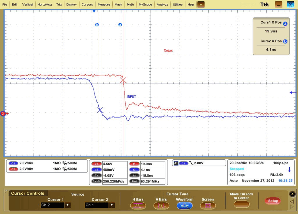 Figure 32. Typical Turnon Waveform
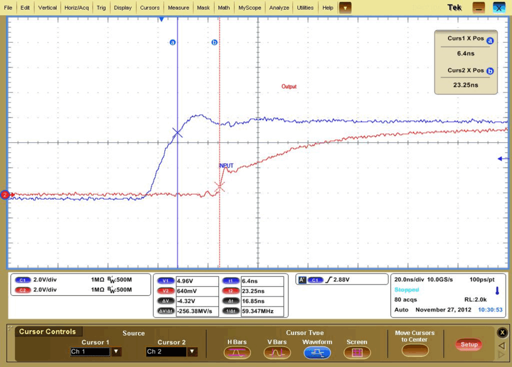 Figure 33. Typical Turnoff Waveform
