ZHCSDP3A December   2014  – May 2015 UCC27528-Q1

PRODUCTION DATA.  

  1. 特性
  2. 应用范围
  3. 说明
  4. 修订历史记录
  5. 说明(续)
  6. Pin Configuration and Functions
  7. Specifications
    1. 7.1 Absolute Maximum Ratings
    2. 7.2 ESD Ratings
    3. 7.3 Recommended Operating Conditions
    4. 7.4 Thermal Information
    5. 7.5 Electrical Characteristics
    6. 7.6 Switching Characteristics
    7. 7.7 Typical Characteristics
  8. Detailed Description
    1. 8.1 Overview
    2. 8.2 Functional Block Diagram
    3. 8.3 Feature Description
      1. 8.3.1 VDD and Undervoltage Lockout
      2. 8.3.2 Operating Supply Current
      3. 8.3.3 Input Stage
      4. 8.3.4 Enable Function
      5. 8.3.5 Output Stage
      6. 8.3.6 Low Propagation Delays and Tightly Matched Outputs
    4. 8.4 Device Functional Modes
  9. Application and Implementation
    1. 9.1 Application Information
    2. 9.2 Typical Application
      1. 9.2.1 Design Requirements
      2. 9.2.2 Detailed Design Procedure
        1. 9.2.2.1 Input-to-Output Logic
        2. 9.2.2.2 Enable and Disable Function
        3. 9.2.2.3 VDD Bias Supply Voltage
        4. 9.2.2.4 Propagation Delay
        5. 9.2.2.5 Drive Current and Power Dissipation
      3. 9.2.3 Application Curves
  10. 10Power Supply Recommendations
  11. 11Layout
    1. 11.1 Layout Guidelines
    2. 11.2 Layout Example
    3. 11.3 Thermal Considerations
  12. 12器件和文档支持
    1. 12.1 商标
    2. 12.2 静电放电警告
    3. 12.3 术语表
  13. 13机械、封装和可订购信息

封装选项

机械数据 (封装 | 引脚)
散热焊盘机械数据 (封装 | 引脚)
订购信息

6 Pin Configuration and Functions

D Package
8-Pin SOIC
Top View
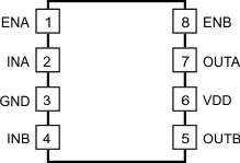
UCC27528-Q1 po_d_8_snvsa89.gif

Pin Functions

PIN I/O DESCRIPTION
NO. NAME
1 ENA I Enable input for Channel A: ENA biased low Disables Channel A output regardless of INA state, ENA biased high or floating Enables Channel A output, ENA allowed to float.
2 INA I Input to Channel A: Non-Inverting Input in UCC27528-Q1, OUTA held low if INA is unbiased or floating.
3 GND Ground: All signals referenced to this pin.
4 INB I Input to Channel B: Non-Inverting Input in UCC27528-Q1, OUTB held low if INB is unbiased or floating.
5 OUTB O Output of Channel B
6 VDD I Bias supply input
7 OUTA O Output of Channel A
8 ENB I Enable input for Channel B: ENB biased low Disables Channel B output regardless of INB state, ENB biased high or floating Enables Channel B output, ENB allowed to float.