ZHCSAO6G December 2012 – June 2019 UCC27531 , UCC27533 , UCC27536 , UCC27537 , UCC27538
PRODUCTION DATA.
- 1 特性
- 2 应用
- 3 说明
- 4 修订历史记录
- 5 Device Comparison Table
- 6 Pin Configuration and Functions
- 7 Specifications
- 8 Detailed Description
-
9 Applications and Implementation
- 9.1 Application Information
- 9.2 Typical Application
- 10Power Supply Recommendations
- 11Layout
- 12器件和文档支持
- 13机械、封装和可订购信息
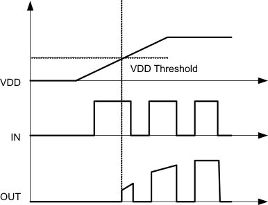
8.3.1 VDD Undervoltage Lockout
The UCC2753x device has internal UVLO protection feature on the VDD pin supply circuit blocks. To ensure acceptable power dissipation in the power switch, this UVLO prevents the operation of the gate driver at low supply voltages. Whenever the driver is in UVLO condition (when VDD voltage less than VON during power up and when VDD voltage is less than VOFF during power down), this circuit holds all outputs LOW, regardless of the status of the inputs. The UVLO is typically 8.9 V with 700-mV typical hysteresis. This hysteresis helps prevent chatter when low VDD supply voltages have noise from the power supply and also when there are droops in the VDD bias voltage when the system commences switching and there is a sudden increase in IDD. The capability to operate at voltage levels such as 10 V to 32 V provides flexibility to drive Si MOSFETs, IGBTs, and emerging SiC FETs.
 Figure 38. Power Up