ZHCSAO4F December 2012 – March 2018 UCC27611
PRODUCTION DATA.
9 Power Supply Recommendations
The bias supply voltage range for which the device is rated to operate is from 4 V to 18 V. The lower end of this range is governed by the internal under voltage-lockout (UVLO) protection feature on the VDD pin supply circuit blocks. Whenever the driver is in UVLO condition when the VDD pin voltage is below the VDD(on) supply start threshold, this feature holds the output low, regardless of the status of the inputs. The upper end of this range is driven by the 20-V absolute maximum voltage rating of the VDD pin of the device (which is a stress rating). Keeping a 2-V margin to allow for transient voltage spikes, the maximum recommended voltage for the VDD pin is 18V.
The UVLO protection feature also involves a hysteresis function. This means that when the VDD pin bias voltage has exceeded the threshold voltage and device begins to operate, and if the voltage drops, then the device continues to deliver normal functionality unless the voltage drop exceeds the hysteresis specification VDD(off). Therefore, ensuring that, while operating at or near the 4-V range, the voltage ripple on the auxiliary power supply output is smaller than the hysteresis specification of the device is important to avoid triggering device shutdown.
During system shutdown, the device operation continues until the VDD pin voltage has dropped below the threshold VDD(off) which must be accounted for while evaluating system shutdown timing design requirements. Likewise, at system startup, the device does not begin operation until the VDD pin voltage has exceeded above the VDD(on) threshold.
Because the driver draws current from the VDD pin to bias all internal circuits, for the best high-speed circuit performance, two VDD bypass capacitors are recommended to prevent noise problems. The use of surface mount components is highly recommended. A 0.1-μF ceramic capacitor must be located as close as possible to the VDD to GND pins of the gate driver. In addition, a larger capacitor (such as 1-μF) with relatively low ESR must be connected in parallel and close proximity to help deliver the high-current peaks required by the load. The parallel combination of capacitors must present a low impedance characteristic for the expected current levels and switching frequencies in the application.
The UCC27611 integrate a LDO to provide well-regulated voltage (VREF) to driving GaN FET. The charge for source current pulses delivered by the OUTH pin is supplied through the VREF pin. As a result, every time a current is sourced out of the OUTH pin a corresponding current pulse is delivered into the device through the VREF pin. Thus ensuring that a local bypass capacitor is provided between the VREF and GND pins and located as close to the device as possible for the purpose of decoupling is important. A low ESR, ceramic surface mount capacitor is necessary.
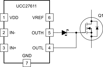
The UCC27611 device is a high-performance driver capable of fast rise and fall times at high-peak currents. Careful PCB layout to reduce parasitic inductances is critical to achieve maximum performance. When a less-than-optimal layout is unavoidable, then TI recommends adding a low capacitance schottky diode to prevent the energy ringing back from the gate and charging up the decoupling capacitor on VREF (see Figure 16).
 Figure 16. Low-Capacitance Schottky Diode to Prevent From Overcharging
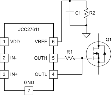
The alternate method would be to add a loading resistor to VREF to bleed off the charge. This method eliminates the additional voltage drop from the diode, but reduces the current available for additional circuits or gate drive if too small a value of resistor is used.
 Figure 17. Load Resistor at VREF to Bleed Off the Charge