ZHCSH10B October 2017 – August 2018 UCC27710
PRODUCTION DATA.
- 1 特性
- 2 应用
- 3 说明
- 4 修订历史记录
- 5 Pin Configuration and Functions
- 6 Specifications
- 7 Detailed Description
-
8 Application and Implementation
- 8.1 Application Information
- 8.2
Typical Application
- 8.2.1 Design Requirements
- 8.2.2
Detailed Design Procedure
- 8.2.2.1 Selecting HI and LI Low Pass Filter Components (RHI, RLI, CHI, CLI)
- 8.2.2.2 Selecting Bootstrap Capacitor (CBOOT)
- 8.2.2.3 Selecting VDD Bypass/Holdup Capacitor (CVDD) and Rbias
- 8.2.2.4 Selecting Bootstrap Resistor (RBOOT)
- 8.2.2.5 Selecting Gate Resistor RON/ROFF
- 8.2.2.6 Selecting Bootstrap Diode
- 8.2.2.7 Estimate the UCC27710 Power Losses (PUCC27710)
- 8.2.2.8 Estimating Junction Temperature
- 8.2.2.9 Operation With IGBT's
- 8.2.3 Application Curves
- 9 Power Supply Recommendations
- 10Layout
- 11器件和文档支持
- 12机械、封装和可订购信息
7.4.2 Output Interlock and Dead Time
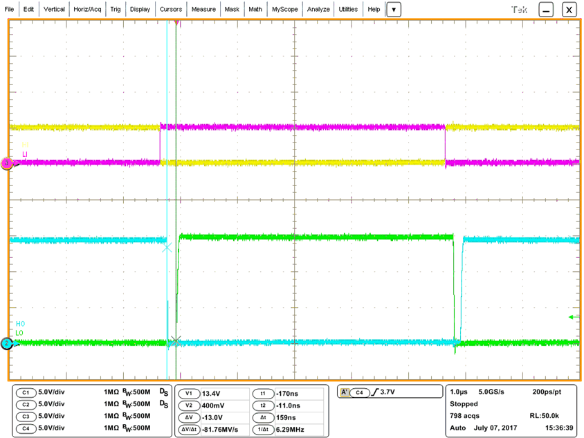
The UCC27710 has cross-conduction prevention logic, which is a feature that does not allow both the high-side and low-side outputs to be in high state simultaneously. In bridge power supply topologies, such as half-bridge or full-bridge, the UCC27710 interlock feature will prevent the high-side and low-side power switches to be turned on simultaneously. The UCC27710 generates a fixed minimum dead time of tDT which is 150 ns nominal in the case of LI and HI overlap or no dead time. Figure 38 illustrates the mode of operation where LI and HI have no dead time and HO and LO outputs have the minimum dead time of tDT.
 Figure 38. HO and LO Minimum Dead Time with LI HI Complementary
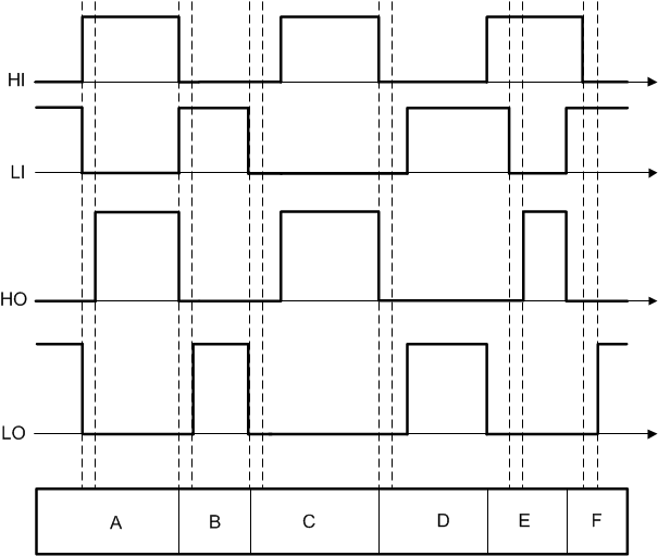
 An input signal's falling edge activates the dead time for the other signal. The output signal's dead time is always set to the longer of either the driver's minimum dead time, tDT, or the input signal's own dead time. If both inputs are high simultaneously, both outputs will immediately be set low. This feature is used to prevent cross conduction, and it does not affect the programmed dead time setting for normal operation. Various driver dead time logic operating conditions are illustrated and explained in Figure 39.
 Figure 39. Input and Output Logic Relationship
 Condition A: HI goes high, LI goes low. LI sets LO low immediately and assigns tDT to HO. HO is allowed to go high after tDT.
Condition B: LI goes high, HI goes low. HI sets HO low immediately and assigns tDT to HO. LO is allowed to go high after tDT.
Condition C: LI goes low, HI is still low. LI sets LO low immediately and assigns tDT to HO. In this case, the input signal's own dead time is longer than tDT. Thus when HI goes high HO is set high immediately.
Condition D: HI goes low, LI is still low. HI sets HO low immediately and assigns tDT to LO. In this case, the input signal's own dead time is longer than tDT. Thus when LI goes high LO is set high immediately.
Condition E: HI goes high, while LI and LO are still high. To avoid cross-conduction, HI immediately sets LO low and keeps HO low. After some time LI goes low and assigns tDT to HO. LO is already low. After tDT HO is allowed to go high.
Condition F: LI goes high, while HI and HO are still high. To avoid cross-conduction, LI immediately sets HO low and keeps LO low. After some time HI goes low and assigns tDT to LO. HO is already low. After tDT LO is allowed to go high.