ZHCSH10B October 2017 – August 2018 UCC27710
PRODUCTION DATA.
- 1 特性
- 2 应用
- 3 说明
- 4 修订历史记录
- 5 Pin Configuration and Functions
- 6 Specifications
- 7 Detailed Description
-
8 Application and Implementation
- 8.1 Application Information
- 8.2
Typical Application
- 8.2.1 Design Requirements
- 8.2.2
Detailed Design Procedure
- 8.2.2.1 Selecting HI and LI Low Pass Filter Components (RHI, RLI, CHI, CLI)
- 8.2.2.2 Selecting Bootstrap Capacitor (CBOOT)
- 8.2.2.3 Selecting VDD Bypass/Holdup Capacitor (CVDD) and Rbias
- 8.2.2.4 Selecting Bootstrap Resistor (RBOOT)
- 8.2.2.5 Selecting Gate Resistor RON/ROFF
- 8.2.2.6 Selecting Bootstrap Diode
- 8.2.2.7 Estimate the UCC27710 Power Losses (PUCC27710)
- 8.2.2.8 Estimating Junction Temperature
- 8.2.2.9 Operation With IGBT's
- 8.2.3 Application Curves
- 9 Power Supply Recommendations
- 10Layout
- 11器件和文档支持
- 12机械、封装和可订购信息
7.4.4 Operation Under Negative HS Voltage Condition
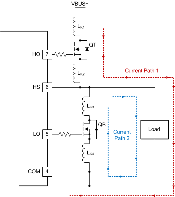
A typical half-bridge configuration with UCC27710 is shown in Figure 40. There are parasitic inductances in the power circuit from die bonding and pinning in QT/QB and PCB tracks of power circuit, the parasitic inductances are labeled LK1,2,3,4.
During switching of HS caused by turning off HO, the current path of power circuit is changed to current path 2 from current path 1. This is known as current commutation. The current across LK3, LK4 and body diode of QB pulls HS lower than COM. The negative voltage of HS with respect to COM causes a logic error of HO if the driver cannot handle negative voltage of HS. However, the UCC27710 offers robust operation under these conditions of negative voltage on HS.
 Figure 40. HS Negative Voltage In Half-Bridge Configuration
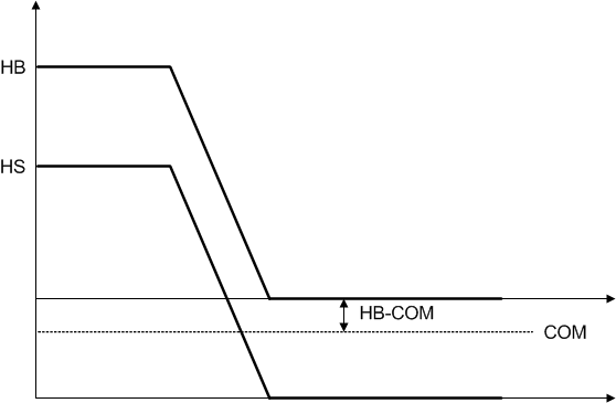
 The level shifter circuit is with respect to COM (refer to Functional Block Diagram), the voltage from HB to COM is the supply voltage of level shifter. Under the condition of HS is negative voltage with respect to COM, the voltage of HB-COM is decreased, as shown in Figure 41. There is a minimum operational supply voltage of level shifter, if the supply voltage of level shifter is too low, the level shifter cannot pass through HI signal to HO. The minimum supply voltage of level shifter of UCC27710 is 4 V, so the recommended HS specification is dependent on HB-HS. The specification of recommended HS is –11 V at HB – HS = 15 V.
In general, HS can operate until -11 V when HB – HS = 15 V as the ESD structure in Figure 35 allows a maximum voltage difference of 20 V between both pins. If HB-HS voltage is different, the minimum HS voltage changes accordingly.
 Figure 41. Level Shifter Supply Voltage with Negative HS
 NOTE
Logic operational for HS of –11 V to 600 V at HB – HS = 15 V
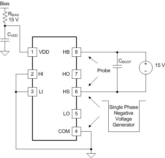
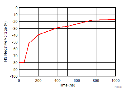
The capability of a typical UCC27710 device to operate under a negative voltage condition in HS pin is reported in Figure 43. The test method is shown in Figure 42.
 Figure 42. Negative Voltage Test Method
  Figure 43. HS Negative Voltage Chart
Pulse Width vs HS Negative Voltage