ZHCSH10B October 2017 – August 2018 UCC27710
PRODUCTION DATA.
- 1 特性
- 2 应用
- 3 说明
- 4 修订历史记录
- 5 Pin Configuration and Functions
- 6 Specifications
- 7 Detailed Description
-
8 Application and Implementation
- 8.1 Application Information
- 8.2
Typical Application
- 8.2.1 Design Requirements
- 8.2.2
Detailed Design Procedure
- 8.2.2.1 Selecting HI and LI Low Pass Filter Components (RHI, RLI, CHI, CLI)
- 8.2.2.2 Selecting Bootstrap Capacitor (CBOOT)
- 8.2.2.3 Selecting VDD Bypass/Holdup Capacitor (CVDD) and Rbias
- 8.2.2.4 Selecting Bootstrap Resistor (RBOOT)
- 8.2.2.5 Selecting Gate Resistor RON/ROFF
- 8.2.2.6 Selecting Bootstrap Diode
- 8.2.2.7 Estimate the UCC27710 Power Losses (PUCC27710)
- 8.2.2.8 Estimating Junction Temperature
- 8.2.2.9 Operation With IGBT's
- 8.2.3 Application Curves
- 9 Power Supply Recommendations
- 10Layout
- 11器件和文档支持
- 12机械、封装和可订购信息
8.2.3 Application Curves
Figure 48 and Figure 49 show the measured LI to LO turn-on and turn-off delay of one UCC27710 device. Channel 3 depicts LI and Channel 4 LO.
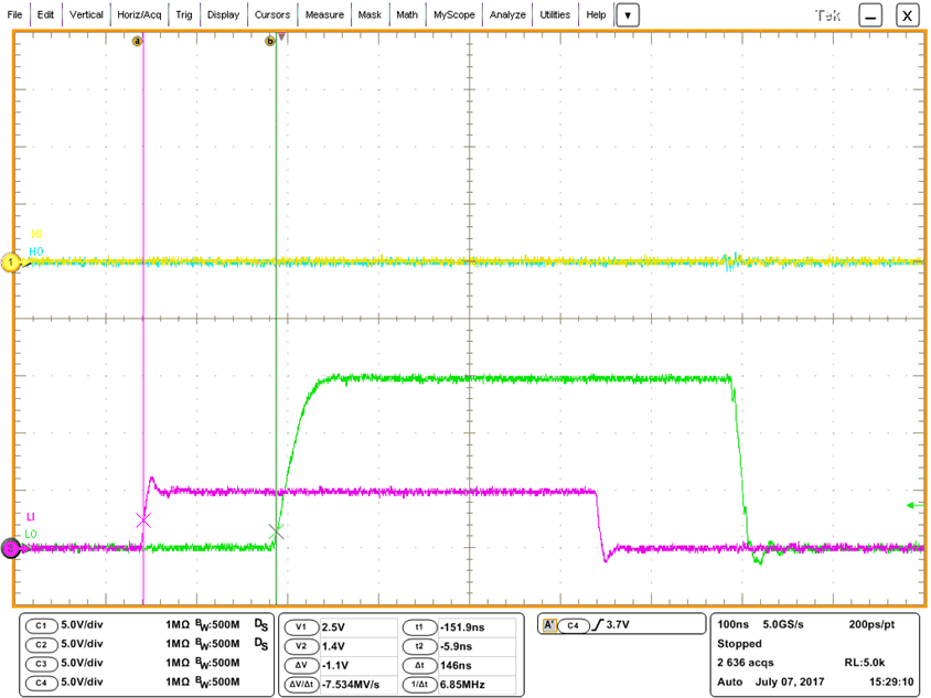 Figure 48. LI to LO Turn-On Propagation Delay
 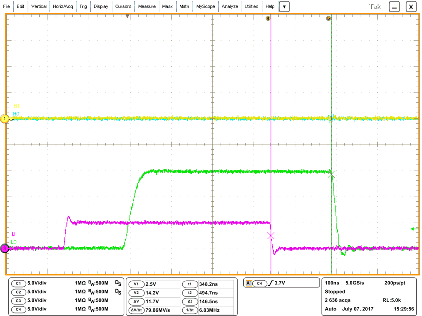 Figure 49. LI to LO Turn-Off Propagation Delay
 Figure 50 and Figure 51 show the measured HI to HO turn-on and turn-off delay of one UCC27710 device. Channel 1 depicts HI and Channel 2 HO.
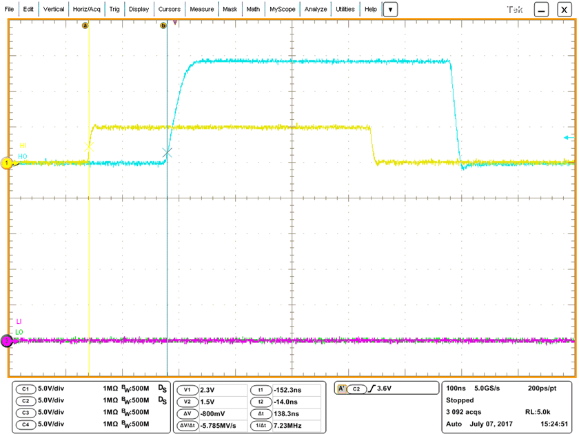 Figure 50. HI to HO Turn-On Propagation Delay
 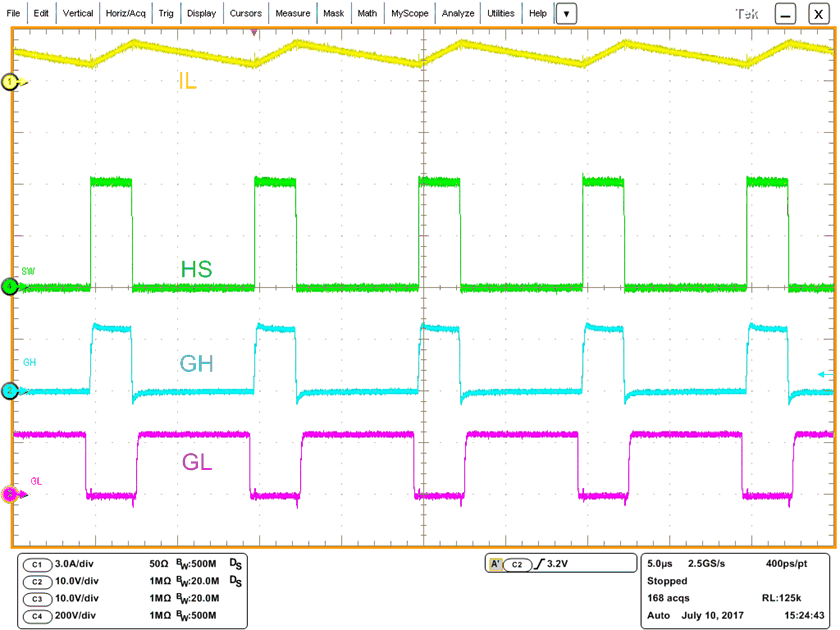 Figure 52. MOSFET Sync-Buck Operating at 400 V and 150 W
 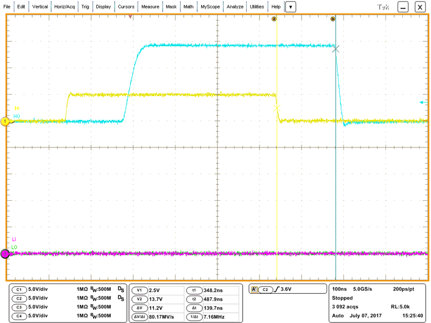 Figure 51. HI to HO Turn-Off Propagation Delay
 Figure 52 shows UCC27710 operating in a high voltage sync-buck. Channel 1 depicts inductor current, Channel 2 high side MOSFET VGS, Channel 3 low side MOSFET VGS, and Channel 4 high voltage switch node.