ZHCSGJ1 August   2017 UCC27712-Q1

PRODUCTION DATA.  

  1. 特性
  2. 应用
  3. 说明
    1.     Device Images
      1.      简化原理图
      2.      典型传播延迟比较
  4. 修订历史记录
  5. Pin Configuration and Functions
    1.     Pin Functions
  6. Specifications
    1. 6.1 Absolute Maximum Ratings
    2. 6.2 ESD Ratings
    3. 6.3 Recommended Operating Conditions
    4. 6.4 Thermal Information
    5. 6.5 Electrical Characteristics
    6. 6.6 Dynamic Electrical Characteristics
    7. 6.7 Typical Characteristics
  7. Detailed Description
    1. 7.1 Overview
    2. 7.2 Functional Block Diagram
    3. 7.3 Feature Description
      1. 7.3.1 VDD and Under Voltage Lockout
      2. 7.3.2 Input and Output Logic Table
      3. 7.3.3 Input Stage
      4. 7.3.4 Output Stage
      5. 7.3.5 Level Shift
      6. 7.3.6 Low Propagation Delays and Tightly Matched Outputs
      7. 7.3.7 Parasitic Diode Structure
    4. 7.4 Device Functional Modes
      1. 7.4.1 Minimum Input Pulse Operation
      2. 7.4.2 Output Interlock and Dead Time
      3. 7.4.3 Operation Under 100% Duty Cycle Condition
      4. 7.4.4 Operation Under Negative HS Voltage Condition
  8. Application and Implementation
    1. 8.1 Application Information
    2. 8.2 Typical Application
      1. 8.2.1 Design Requirements
      2. 8.2.2 Detailed Design Procedure
        1. 8.2.2.1 Selecting HI and LI Low Pass Filter Components (RHI, RLI, CHI, CLI)
        2. 8.2.2.2 Selecting Bootstrap Capacitor (CBOOT)
        3. 8.2.2.3 Selecting VDD Bypass/Holdup Capacitor (CVDD) and Rbias
        4. 8.2.2.4 Selecting Bootstrap Resistor (RBOOT)
        5. 8.2.2.5 Selecting Gate Resistor RON/ROFF
        6. 8.2.2.6 Selecting Bootstrap Diode
        7. 8.2.2.7 Estimate the UCC27712-Q1 Power Losses (PUCC27712-Q1)
        8. 8.2.2.8 Estimating Junction Temperature
        9. 8.2.2.9 Operation With IGBT's
      3. 8.2.3 Application Curves
  9. Power Supply Recommendations
  10. 10Layout
    1. 10.1 Layout Guidelines
    2. 10.2 Layout Example
  11. 11器件和文档支持
    1. 11.1 文档支持
      1. 11.1.1 相关文档
    2. 11.2 相关链接
    3. 11.3 社区资源
    4. 11.4 商标
    5. 11.5 静电放电警告
    6. 11.6 Glossary
  12. 12机械、封装和可订购信息

封装选项

机械数据 (封装 | 引脚)
散热焊盘机械数据 (封装 | 引脚)
订购信息

Typical Characteristics
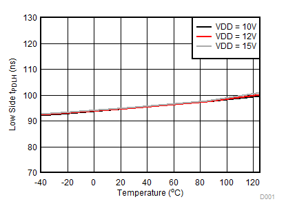
UCC27712-Q1 D001_slusce9.gif
Figure 2. Low-Side, Turn-On Propagation Delay vs Temperature
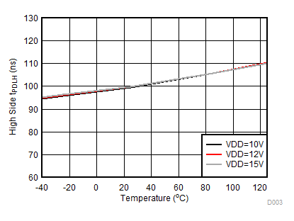
UCC27712-Q1 D003_slusce9.gif
Figure 4. High-Side, Turn-On Propagation Delay vs Temperature
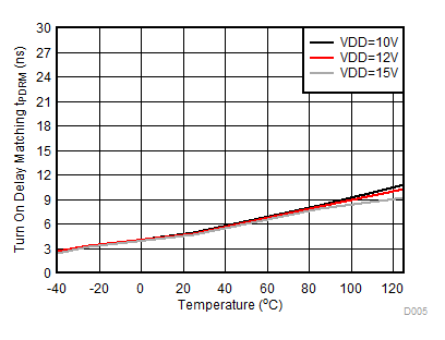
UCC27712-Q1 D005_slusce9.gif
Figure 6. Turn-On Delay Matching vs Temperature
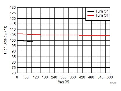
UCC27712-Q1 d007new_slusce9.gif
Figure 8. High-Side Propagation Delay vs HS
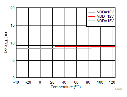
UCC27712-Q1 D009_slusce9.gif
Figure 10. LO Fall Time with 1000-pF Load vs Temperature
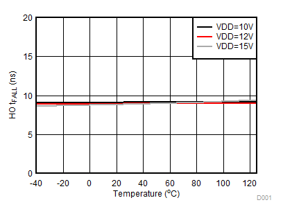
UCC27712-Q1 D0011_slusce9.gif
Figure 12. HO Fall Time with 1000-pF Load vs Temperature
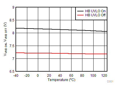
UCC27712-Q1 D0013_slusce9.gif
Figure 14. VHB-VHS UVLO Thresholds vs Temperature
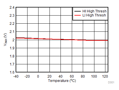
UCC27712-Q1 D0015_slusce9.gif
Figure 16. HI/LI Pin High Threshold vs Temperature
UCC27712-Q1 D0017_slusce9.gif
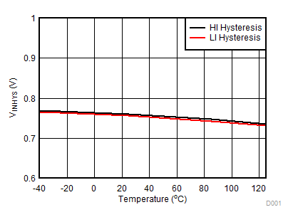
Figure 18. HI/LI Pin Hysteresis vs Temperature
UCC27712-Q1 D0019_slusce9.gif
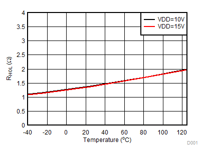
Figure 20. HO Output Pull-Down Resistance vs Temperature
UCC27712-Q1 D0021_slusce9.gif
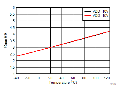
Figure 22. HO Output Pull-Up Resistance vs Temperature
UCC27712-Q1 D0023_slusce9.gif
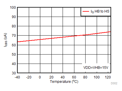
Figure 24. Quiescent HB to HS Supply Current vs Temperature
UCC27712-Q1 D0025_slusce9.gif
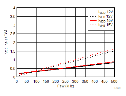
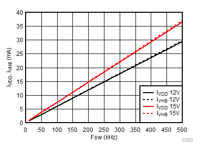
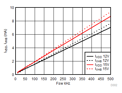
Figure 26. VDD and HB Operating Current with No Load vs Switching Frequency
UCC27712-Q1 D0027_slusce9.gif
Figure 28. VDD and HB Operating Current with 4700-pF Load vs Switching Frequency
UCC27712-Q1 D002_slusce9.gif
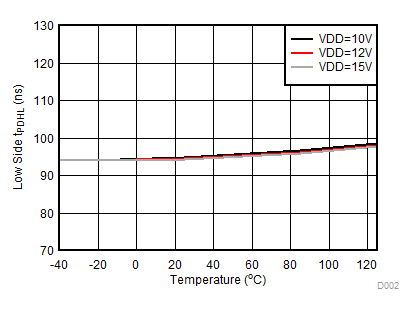
Figure 3. Low-Side, Turn-Off Propagation Delay vs Temperature
UCC27712-Q1 D004_slusce9.gif
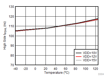
Figure 5. High-Side, Turn-Off Propagation Delay vs Temperature
UCC27712-Q1 D006_slusce9.gif
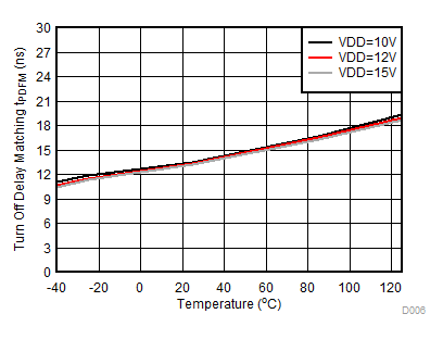
Figure 7. Turn-Off Delay Matching vs Temperature
UCC27712-Q1 D008_slusce9.gif
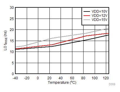
Figure 9. LO Rise Time with 1000-pF Load vs Temperature
UCC27712-Q1 D0010_slusce9.gif
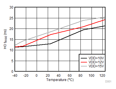
Figure 11. HO Rise Time with 1000-pF Load vs Temperature
UCC27712-Q1 D0012_slusce9.gif
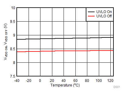
Figure 13. VDD UVLO Thresholds vs Temperature
UCC27712-Q1 D0014_slusce9.gif
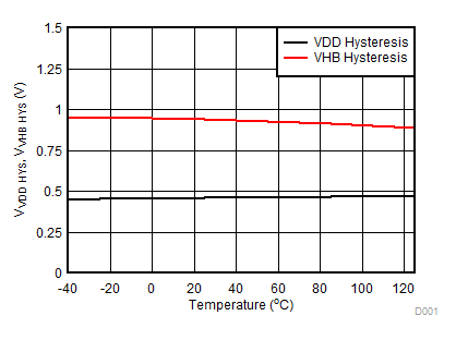
Figure 15. VDD and VHB-VHS UVLO Hysteresis vs Temperature
UCC27712-Q1 D0016_slusce9.gif
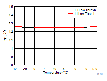
Figure 17. HI/LI Pin Low Threshold vs Temperature
UCC27712-Q1 D0018_slusce9.gif
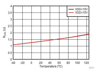
Figure 19. LO Output Pull-Down Resistance vs Temperature
UCC27712-Q1 D0020_slusce9.gif
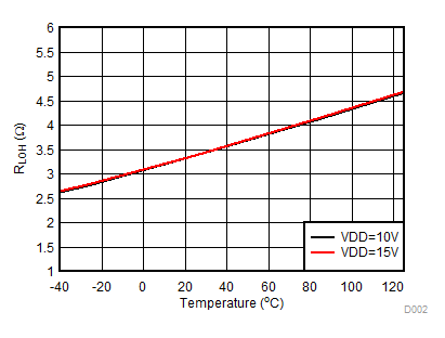
Figure 21. LO Output Pull-Up Resistance vs Temperature
UCC27712-Q1 D0022_slusce9.gif
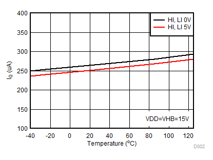
Figure 23. Total Quiescent VDD plus HB Supply Current vs Temperature
UCC27712-Q1 D0024_slusce9.gif
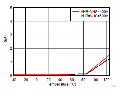
Figure 25. HB to COM Bootstrap Supply Leakage Current vs Temperature
UCC27712-Q1 D0026_slusce9.gif
Figure 27. VDD and HB Operating Current with 1000-pF Load vs Switching Frequency