ZHCSGJ1 August 2017 UCC27712-Q1
PRODUCTION DATA.
- 1 特性
- 2 应用
- 3 说明
- 4 修订历史记录
- 5 Pin Configuration and Functions
- 6 Specifications
- 7 Detailed Description
-
8 Application and Implementation
- 8.1 Application Information
- 8.2
Typical Application
- 8.2.1 Design Requirements
- 8.2.2
Detailed Design Procedure
- 8.2.2.1 Selecting HI and LI Low Pass Filter Components (RHI, RLI, CHI, CLI)
- 8.2.2.2 Selecting Bootstrap Capacitor (CBOOT)
- 8.2.2.3 Selecting VDD Bypass/Holdup Capacitor (CVDD) and Rbias
- 8.2.2.4 Selecting Bootstrap Resistor (RBOOT)
- 8.2.2.5 Selecting Gate Resistor RON/ROFF
- 8.2.2.6 Selecting Bootstrap Diode
- 8.2.2.7 Estimate the UCC27712-Q1 Power Losses (PUCC27712-Q1)
- 8.2.2.8 Estimating Junction Temperature
- 8.2.2.9 Operation With IGBT's
- 8.2.3 Application Curves
- 9 Power Supply Recommendations
- 10Layout
- 11器件和文档支持
- 12机械、封装和可订购信息
7.4.1 Minimum Input Pulse Operation
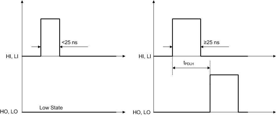
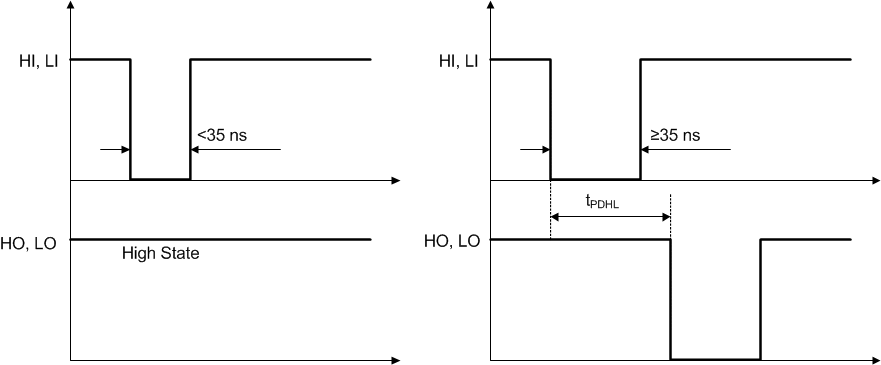
The UCC27712-Q1 device has a minimum turn-on, turn-off pulse transfer function to the output pin from the input pin. This function ensures UCC27712-Q1 is in the correct state when the input signal is very narrow. The function is summarized in Figure 36 and Figure 37. The tON which is 25 ns typical is shown in Figure 36 and tOFF which is 35ns typical is shown in Figure 37
 Figure 36. Minimum Turn-On Pulse
 Figure 37. Minimum Turn-Off Pulse