ZHCSGJ1 August 2017 UCC27712-Q1
PRODUCTION DATA.
- 1 特性
- 2 应用
- 3 说明
- 4 修订历史记录
- 5 Pin Configuration and Functions
- 6 Specifications
- 7 Detailed Description
-
8 Application and Implementation
- 8.1 Application Information
- 8.2
Typical Application
- 8.2.1 Design Requirements
- 8.2.2
Detailed Design Procedure
- 8.2.2.1 Selecting HI and LI Low Pass Filter Components (RHI, RLI, CHI, CLI)
- 8.2.2.2 Selecting Bootstrap Capacitor (CBOOT)
- 8.2.2.3 Selecting VDD Bypass/Holdup Capacitor (CVDD) and Rbias
- 8.2.2.4 Selecting Bootstrap Resistor (RBOOT)
- 8.2.2.5 Selecting Gate Resistor RON/ROFF
- 8.2.2.6 Selecting Bootstrap Diode
- 8.2.2.7 Estimate the UCC27712-Q1 Power Losses (PUCC27712-Q1)
- 8.2.2.8 Estimating Junction Temperature
- 8.2.2.9 Operation With IGBT's
- 8.2.3 Application Curves
- 9 Power Supply Recommendations
- 10Layout
- 11器件和文档支持
- 12机械、封装和可订购信息
8.2.2.3 Selecting VDD Bypass/Holdup Capacitor (CVDD) and Rbias
The VDD capacitor (CVDD) should be chosen to be at least 10 times larger than CBOOT so there is minimal voltage drop on the VDD capacitor when charging the boot capacitor . For this design example a 4.7-µF capacitor was selected.
Equation 4. 

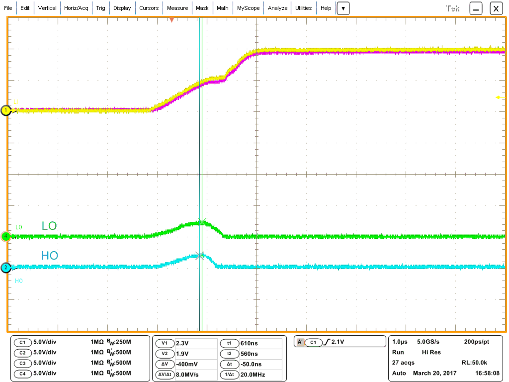
A 10-Ω resistor RBIAS in series with bias supply and VDD pin is recommended to make the VDD ramp up time larger than 20 µs to minimize LO and HO rising as shown in Figure 45
 Figure 45. VDD/HB-HS Fast Ramp Up