ZHCSGJ1 August 2017 UCC27712-Q1
PRODUCTION DATA.
- 1 特性
- 2 应用
- 3 说明
- 4 修订历史记录
- 5 Pin Configuration and Functions
- 6 Specifications
- 7 Detailed Description
-
8 Application and Implementation
- 8.1 Application Information
- 8.2
Typical Application
- 8.2.1 Design Requirements
- 8.2.2
Detailed Design Procedure
- 8.2.2.1 Selecting HI and LI Low Pass Filter Components (RHI, RLI, CHI, CLI)
- 8.2.2.2 Selecting Bootstrap Capacitor (CBOOT)
- 8.2.2.3 Selecting VDD Bypass/Holdup Capacitor (CVDD) and Rbias
- 8.2.2.4 Selecting Bootstrap Resistor (RBOOT)
- 8.2.2.5 Selecting Gate Resistor RON/ROFF
- 8.2.2.6 Selecting Bootstrap Diode
- 8.2.2.7 Estimate the UCC27712-Q1 Power Losses (PUCC27712-Q1)
- 8.2.2.8 Estimating Junction Temperature
- 8.2.2.9 Operation With IGBT's
- 8.2.3 Application Curves
- 9 Power Supply Recommendations
- 10Layout
- 11器件和文档支持
- 12机械、封装和可订购信息
8.2.2.9 Operation With IGBT's
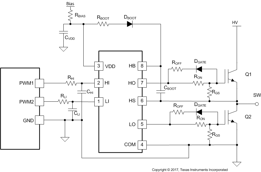
The UCC27712-Q1 is well suited for driving IGBT's in various applications including motor drive and inverters. The design procedure is as the previous MOSFET example but the VDD voltage is typically 15-V to drive IGBT devices. Use the power transistor parameters and application specifications to determine the detail design and component values. See Figure 46 below for a typical IGBT application.
 Figure 46. Typical IGBT Application Schematic
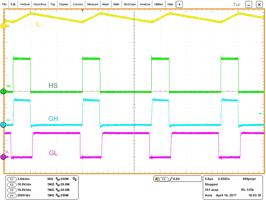
Refer to Figure 47 below for the UCC27712-Q1 driving 40-A, 650-V IGBT's in a high voltage sync buck configuration. The input voltage is 400 V, output 100 V with a 150-W output load. Channel 1 is the inductor current, Channel 2 is high-side IGBT VGE, Channel 3 is low-side IGBT VGE, and Channel 4 is the switch node or HS voltage.
 Figure 47. IGBT Sync-Buck Operating at 400 V and 150 W