ZHCSE29A August 2015 – August 2015 UCC27714
PRODUCTION DATA.
- 1 特性
- 2 应用
- 3 说明
- 4 简化电路原理图
- 5 修订历史记录
- 6 Pin Configuration and Functions
- 7 Specifications
- 8 Detailed Description
-
9 Application and Implementation
- 9.1 Application Information
- 9.2
Typical Application
- 9.2.1 Design Requirements
- 9.2.2
Detailed Design Procedure
- 9.2.2.1 Selecting HI and LI Low Pass Filter Components (RHI, RLI, CHI, CLI)
- 9.2.2.2 Selecting Bootstrap Capacitor (CBOOT)
- 9.2.2.3 Selecting VDD Bypass/Holdup Capacitor (CVDD) and Rbias
- 9.2.2.4 Selecting Bootstrap Resistor (RBOOT)
- 9.2.2.5 Selecting Gate Resistor RHO/RLO
- 9.2.2.6 Selecting Bootstrap Diode
- 9.2.2.7 Estimate the UCC27714 Power Losses (PUCC27714)
- 9.2.2.8 Application Example Schematic Note
- 9.2.3 Application Curves
- 10Power Supply Recommendations
- 11Layout
- 12器件和文档支持
- 13机械、封装和可订购信息
8 Detailed Description
8.1 Overview
High-current, gate-driver devices are required in switching power applications for a variety of reasons. In order to implement fast switching of power devices and reduce associated switching power losses, a powerful gate-driver device is employed between the PWM output of control devices and the gates of the power semiconductor devices. Further, gate-driver devices are indispensable when having the PWM controller device directly drive the gates of the switching devices is sometimes not feasible. In the case of digital power supply controllers, this situation is often encountered because the PWM signal from the digital controller is often a 3.3-V logic signal which is not capable of effectively turning on a power switch.
In bridge topologies, like hard-switch half bridge, hard-switch full bridge, half-bridge and full-bridge LLC, phase-shift full bridge, 2-transistor forward, the source and emitter pin of the top-side power MOSFET and IGBT switch is referenced to a node whose voltage changes dynamically; that is, not referenced to a fixed potential, so floating-driver devices are necessary in these topologies.
The UCC27714 is a high-side and low-side driver dedicated for offline AC-to-DC power supplies and inverters. The high side is a floating driver that can be biased effectively using a bootstrap circuit, and can handle up to 600-V. The driver includes an enable and disable function, and can be used with 100% duty cycle as long as HB-HS can be above UVLO of the high side.
The device features industry best-in-class propagation delays and delay matching between both channels aimed at minimizing pulse distortion in high-frequency switching applications. Each channel is controlled by its respective input pins (HI and LI), allowing full and independent flexibility to control on and off state of the output. The UCC27714 includes protection features wherein the outputs are held low when inputs are floating or when the minimum input pulse width specification is not met. The driver inputs are CMOS and TTL compatible for easy interface to digital power controllers and analog controllers alike. An optional enable and disable function is included in Pin 4 of the UCC27714. The pin is internally pulled to VDD for active-high logic and can be left open (NC) for standard operation when outputs are enable by default. If the pin is pulled to GND, then outputs are disabled.
8.2 Functional Block Diagram
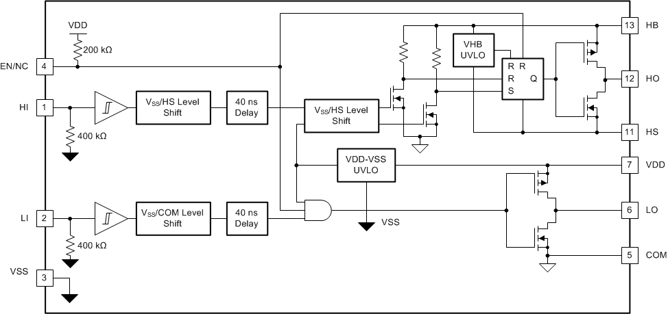 Figure 38. UCC27714 Block Diagram
8.3 Feature Description
8.3.1 VDD and Under Voltage Lockout
The UCC27714 has an internal under voltage-lockout (UVLO) protection feature on the supply circuit blocks between VDD and VSS pins, as well as between HB and HS pins. When VDD bias voltage is lower than the VVDD(on) threshold at device start-up or lower than VVDD(off) after start-up, the VDD UVLO feature holds both the LO and HO outputs LOW, regardless of the status of the HI and LI inputs. On the other hand, if HB-HS bias supply voltage is lower than the VVHB(on) threshold at start-up or VVHB(off) after start-up, the HB-HS UVLO feature only holds HO to LOW, regardless of the status of the HI. The LO output status is not affected by the HB-HS UVLO feature (see Table 1 and Table 2). This allows the LO output to turn-on and re-charge the HB-HS capacitor using the boot-strap circuit and thus allows HB-HS bias voltage to surpass the VVHB(on) threshold.
Both the VDD and VHB UVLO protection functions are provided with a hysteresis feature. This hysteresis prevents chatter when there is ground noise from the power supply. Also this allows the device to accept a small drop in the bias voltage which is bound to happen when the device starts switching and quiescent current consumption increases instantaneously, as well as when the boot-strap circuit charges the HB-HS capacitor during the first instance of LO turn-on causing a drop in VDD voltage.
The UVLO circuit of VDD-VSS and HB-HS in UCC27714 generate internal signals to enable/disable the outputs after UVLO_ON/UVLO_OFF thresholds are crossed respectively (please refer to Figure 39). Design considerations indicate that the UVLO propagation delay before the outputs are enabled and disabled can vary from 10 μs to 70 μs.
Special attention must be paid to the situation when the VDD-VSS voltage drops rapidly, during abnormal condition tests such as pin-to-pin shorting. If VDD-VSS voltage drops from VDD(OFF) to a 4-V level in a time that is less than the propagation delay, then there is a chance for the HO and LO outputs to be latched in the incumbent state prior to the UVLO incident. For UVLO_OFF logic block to be effective in turning off the outputs, the VDD-VSS bias voltage must be at least 4 V. Hence, it is recommended that VDD pin voltage is not allowed to dip from VDD(OFF) to 4 V in 70 μs or less.
Table 1. VDD UVLO Feature Logic Operation
| CONDITION (VHB-VHS>VVHB, ON FOR ALL CASES BELOW) | HI | LI | HO | LO |
|---|---|---|---|---|
| VDD-VSS < VVDD(on) during device start up | H | L | L | L |
| VDD-VSS < VVDD(on) during device start up | L | H | L | L |
| VDD-VSS < VVDD(on) during device start up | H | H | L | L |
| VDD-VSS < VVDD(on) during device start up | L | L | L | L |
| VDD-VSS < VVDD(off) after device start up | H | L | L | L |
| VDD-VSS < VVDD(off) after device start up | L | H | L | L |
| VDD-VSS < VVDD(off) after device start up | H | H | L | L |
| VDD-VSS < VVDD(off) after device start up | L | L | L | L |
Table 2. VHB UVLO Feature Logic Operation
| CONDITION (VDD-VSS > VVDD,ON FOR ALL CASES BELOW) | HI | LI | HO | LO |
|---|---|---|---|---|
| VHB-VHS < VVHB(on) during device start up | H | L | L | L |
| VHB-VHS < VVHB(on) during device start up | L | H | L | H |
| VHB-VHS < VVHB(on) during device start up | H | H | L | H |
| VHB-VHS < VVHB(on) during device start up | L | L | L | L |
| VHB-VHS < VVHB(off) after device start up | H | L | L | L |
| VHB-VHS < VVHB(off) after device start up | L | H | L | H |
| VHB-VHS < VVHB(off) after device start up | H | H | L | H |
| VHB-VHS < VVHB(off) after device start up | L | L | L | L |
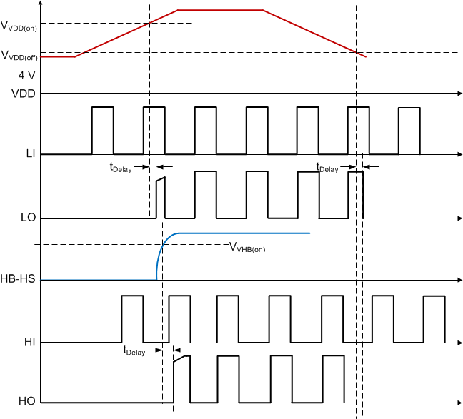 Figure 39. Power-Up Driver
8.3.2 Input and Output Logic Table
UCC27714 features independent inputs, HI and LI, for controlling the state of the outputs, HO and LO, respectively. The device does not include internal cross-conduction prevention logic and allows both HO and LO outputs to be turned on simultaneously (refer to Table 3). This feature allows it to be used topologies such as 2-transistor forward.
Table 3. Input/Output Logic Table (1)
(Assuming no UVLO fault condition exists for VDD and VHB)
| EN/NC | HI | LI | HO | LO |
|---|---|---|---|---|
| H | L | L | L | L |
| H | L | H | L | H |
| H | H | L | H | L |
| H | H | H | H | H |
| L | Any | Any | L | L |
| Any | × | × | L | L |
| × | L | L | L | L |
| × | L | H | L | H |
| × | H | L | H | L |
| × | H | H | H | H |
8.3.3 Input Stage
The input pins of UCC27714 are based on a TTL and CMOS compatible input-threshold logic that is independent of the VDD supply voltage. With typical high threshold (VINH) of 2.3 V and typical low threshold (VINL) of 1.6 V, along with very little temperature variation as summarized in Figure 20 and Figure 21, the input pins are conveniently driven with logic level PWM control signals derived from 3.3-V and 5-V digital power-controller devices. Wider hysteresis (typically 0.7 V) offers enhanced noise immunity compared to traditional TTL logic implementations, where the hysteresis is typically less than 0.5 V. UCC27714 also features tight control of the input pin threshold voltage levels which eases system design considerations and ensures stable operation across temperature.
The UCC27714 includes an important feature: wherein, whenever any of the input pins is in a floating condition, the output of the respective channel is held in the low state. This is achieved using GND pull-down resistors on all the input pins (HI, LI), the input impedance of the input pins (HI, LI) is 400-kΩ typically, as shown in the device block diagrams.
The UCC27714 input pins are capable of sustaining voltages higher than the bias voltage applied on the VDD pin of the device, as long as the absolute magnitude is less than the recommended operating condition's maximum ratings. This features offers the convenience of driving the PWM controller at a higher VDD bias voltage than the UCC27714 helping to reduce gate charge related switching losses. This capability is envisaged in UCC27714 by way of two ESD diodes tied back-to-front as shown in Figure 40.
Additionally, the input pins are also capable of sustaining negative voltages below VSS, as long as the magnitude of the negative voltage is less than the recommended operating condition minimum ratings. A similar diode arrangement exists between the input pins and VSS as illustrated in Figure 40.
The input stage of each driver must be driven by a signal with a short rise or fall time. This condition is satisfied in typical power supply applications, when the input signals are provided by a PWM controller or logic gates with fast transition times. With a slow changing input voltage, the output of driver may switch repeatedly at a high frequency. While the wide hysteresis offered in UCC27714 definitely alleviates this concern over most other TTL input threshold devices, extra care is necessary in these implementations. If limiting the rise or fall times to the power device is the primary goal, then an external resistance is highly recommended between the output of the driver and the power device. This external resistor has the additional benefit of reducing part of the gate-charge related power dissipation in the gate-driver device package and transferring it into the external resistor itself. If an RC filter is to be added on the input pins for reducing the impact of system noise and ground bounce, the time constant of the RC filter must be 20 ns or less, for example, 50 Ω with 220 pF is an acceptable choice.
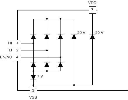 Figure 40. Diode Structure of Input Stage
8.3.4 Output Stage
The UCC27714 device output stage features a unique architecture on the pull up structure which delivers the highest peak-source current when it is most needed during the Miller plateau region of the power-switch turn on transition (when the power switch drain or collector voltage experiences dV/dt). The output stage pull-up structure features a P-Channel MOSFET and an additional N-Channel MOSFET in parallel. The function of the N-Channel MOSFET is to provide a brief boost in the peak sourcing current enabling fast turn on. This is accomplished by briefly turning-on the N-Channel MOSFET during a narrow instant when the output is changing state from low to high.
The ROH parameter (see Electrical Characteristics) is a DC measurement and it is representative of the on-resistance of the P-Channel device only. This is because the N-Channel device is held in the off state in DC condition and is turned on only for a narrow instant when output changes state from low to high.
NOTE
The effective resistance of UCC27714 pull-up stage during the turn-on instant is much lower than what is represented by ROH parameter.
The pull-down structure in UCC27714 is simply composed of a N-Channel MOSFET. The ROL parameter (see Electrical Characteristics), which is also a DC measurement, is representative of the impedance of the pull-down stage in the device.
Each output stage in UCC27714 is capable of supplying 4-A peak source and 4-A peak sink current pulses. The output voltage swings between (VDD and COM) / (HB and HS) providing rail-to-rail operation, thanks to the MOS-out stage which delivers very low drop-out. The low drop-out voltage is summarized in Figure 23, Figure 24, Figure 25 and Figure 26
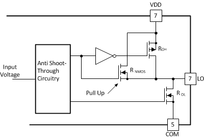 Figure 41. Output Stage Structure
8.3.5 Level Shift
The level shift circuit (refer to the Functional Block Diagram) is the interface from the high-side input to the high-side driver stage which is referenced to the switch node (HS). It is a pulsed generated level shifter. With an input signal the pulse generator generates "on" pulses based on the rising edge of the signal and "off" pulses based on the falling edge. On pulses and off pulses turn on each branch of the level shifter so that current flows in each branch to generate different voltages, which is transferred to the set and reset signal in the high side. The signal is rebuilt by the RS latch in the high side domain. The level shift allows control of the HO output referenced to the HS pin and provides excellent delay matching with the low-side driver. The delay matching of UCC27714 is summarized in Figure 6 and Figure 7.
The level shifter in UCC27714 offers best-in-class capability while operating under negative voltage conditions on HS pin. The level shifter is able to transfer signals from the HI input to HO output with only 4-V headroom between HB and COM. Refer to Operation Under Negative HS Voltage Condition for detailed explanations.
8.3.6 Low Propagation Delays and Tightly Matched Outputs
The UCC27714 features a best in class, 90-ns (typical) propagation delay (refer to Figure 2, Figure 3, Figure 4 and Figure 5 ) between input and output in high voltage 600-V driver, which goes to offer the lowest level of pulse-transmission distortion available in the industry for high frequency switching applications.
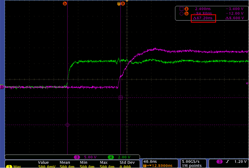 Figure 42. Turn-On Propagation Delay
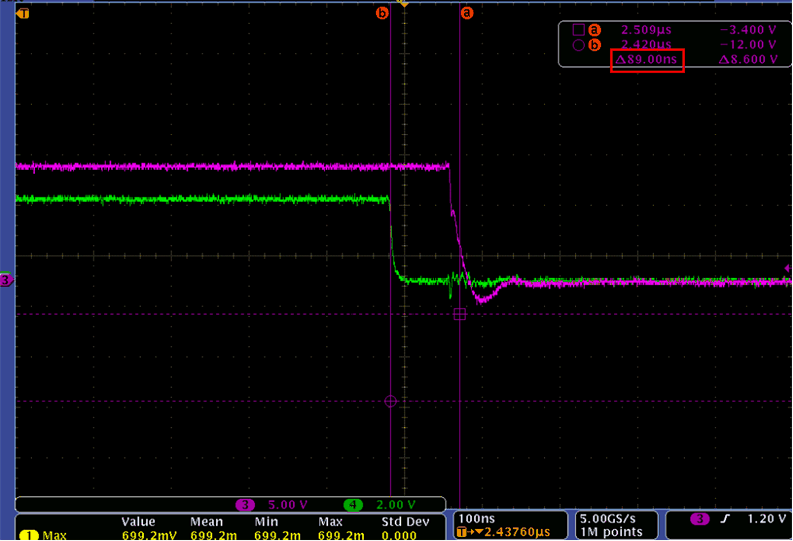 Figure 43. Turn-Off Propagation Delay
8.3.7 Parasitic Diode Structure in UCC27714
Figure 44 illustrates the multiple parasitic diodes involved in the ESD protection components of UCC27714 device. This provides a pictorial representation of the absolute maximum rating for the device.
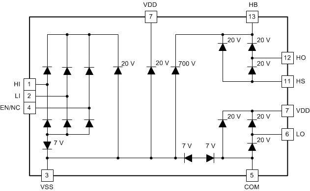 Figure 44. ESD Structure
8.4 Device Functional Modes
8.4.1 Enable Function
The enable function is an extremely beneficial feature in applications where the DC-to-DC controller is located on the secondary side, which is very common with digital controllers. In these applications, it is easy to turn off the driver signal in a very short time when critical faults such as primary-side overcurrent occurs. The Enable Function response time is typically around 80 ns, refer to Figure 31, Figure 32 and Figure 45.
The enable pin controls both the high-side and low-side driver-channel operation. The enable pin is based on a non-inverting configuration (active-high operation). Thus, when EN pin is driven high the driver is enabled and when EN pin is driven low the driver outputs are low. The EN pin is internally pulled up to VDD using 200-kΩ, pull-up resistor as a result of which the outputs of the device are enabled in the default state. The EN pin is left floating or Not Connected (N/C) for standard operation, where the enable feature is not needed. Care must be taken not to connect the EN pin to ground, which permanently disables the device. Like the input pins, the enable pin is also based on a TTL and CMOS compatible input-threshold logic that is independent of the supply voltage and is effectively controlled using logic signal from 3.3-V and 5-V microcontrollers. The UCC27714 also features tight control of the enable-function-threshold voltage levels which eases system design considerations and ensures stable operation across temperature (refer to Figure 20 and Figure 21).
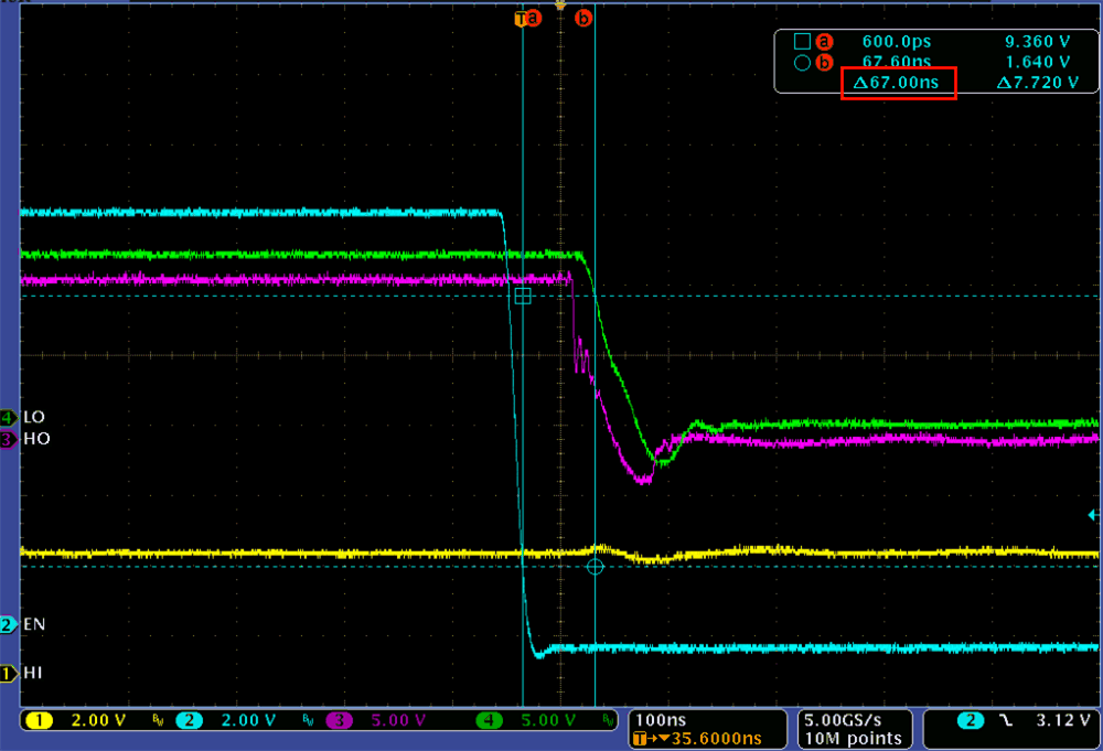 Figure 45. EN Function Response Time
8.4.2 Minimum Input Pulse Operation
The UCC27714 device has a minimum turn-on, turn-off pulse transfer function to the output pin from the input pin. This function ensures UCC27714 is in the correct state when the input signal is very narrow. The function is summarized in Figure 46 and Figure 47. The 100 ns shown in Figure 46 and Figure 47 is ensured by design.
The tON and tOFF parameters in the electrical table are characterized by applying a 100-ns wide input pulses and monitoring for a corresponding change of state in the outputs.
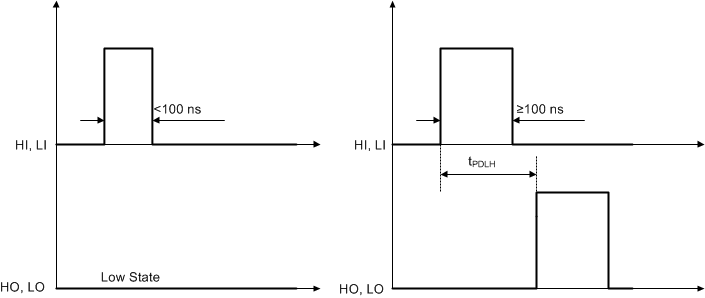 Figure 46. Minimum Turn-On Pulse
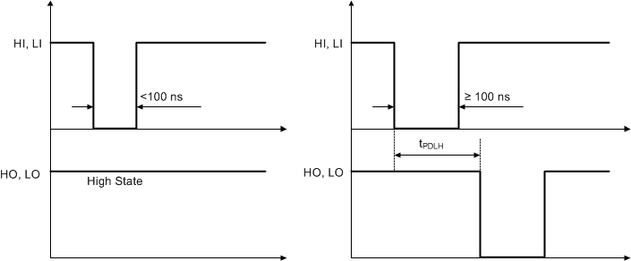 Figure 47. Minimum Turn-Off Pulse
8.4.3 Operation with HO and LO Outputs High Simultaneously
The UCC27714 does not have cross-conduction prevention logic, which is a feature that does not allow both the high-side and low-side outputs to be in high state simultaneously. In some power supply topologies, such as two-transistor forward, it is required for both the high-side and low-side power switches to be turned on simultaneously. The UCC27714 can handle both HO and LO high condition at same time as long as there are no bias supply UVLO fault conditions present. Figure 48 illustrates the mode of operation where both HO and LO outputs are in high state.
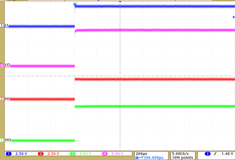 Figure 48. Simultaneously Supported HO and LO High State
The circuit in Figure 49 shows a two-transistor forward converter circuit driven by the UCC27714. This circuit requires both outputs to be high or low simultaneously. The bootstrap capacitor would be charged with LO high state only (HO low). As this would decrease overall system efficiency two additional diode and two additional transistors are required to charge the bootstrap capacitor during LO and HO low period.
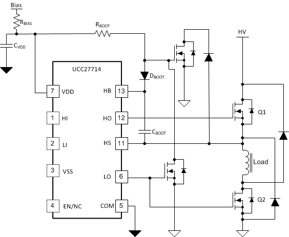 Figure 49. Two-Transistor Forward Converter Circuit
8.4.4 Operation Under 100% Duty Cycle Condition
The UCC27714 allows constant on or constant off operation (0% and/or 100% duty cycle) as long as the VDD and VHB bias supplies are maintained above the UVLO thresholds. This is a challenge when boot-strap supplies are used for VHB. However, when a dedicated bias supply is used, constant on or constant off conditions can be supported, refer to Figure 48.
8.4.5 Operation Under Negative HS Voltage Condition
A typical half-bridge configuration with UCC27714 is shown in Figure 50. There are parasitic inductances in the power circuit from die bonding and pinning in QT/QB and PCB tracks of power circuit, the parasitic inductances are labeled LK1,2,3,4.
During switching of HS caused by turning off HO, the current path of power circuit is changed to current path 2 from current path 1. This is known as current commutation. The current across LK3, LK4 and body diode of QB pulls HS lower than COM, like shown in the waveform in Figure 50. The negative voltage of HS with respect to COM causes a logic error of HO if the driver cannot handle negative voltage of HS. However, the UCC27724 offers robust operation under these conditions of negative voltage on HS.
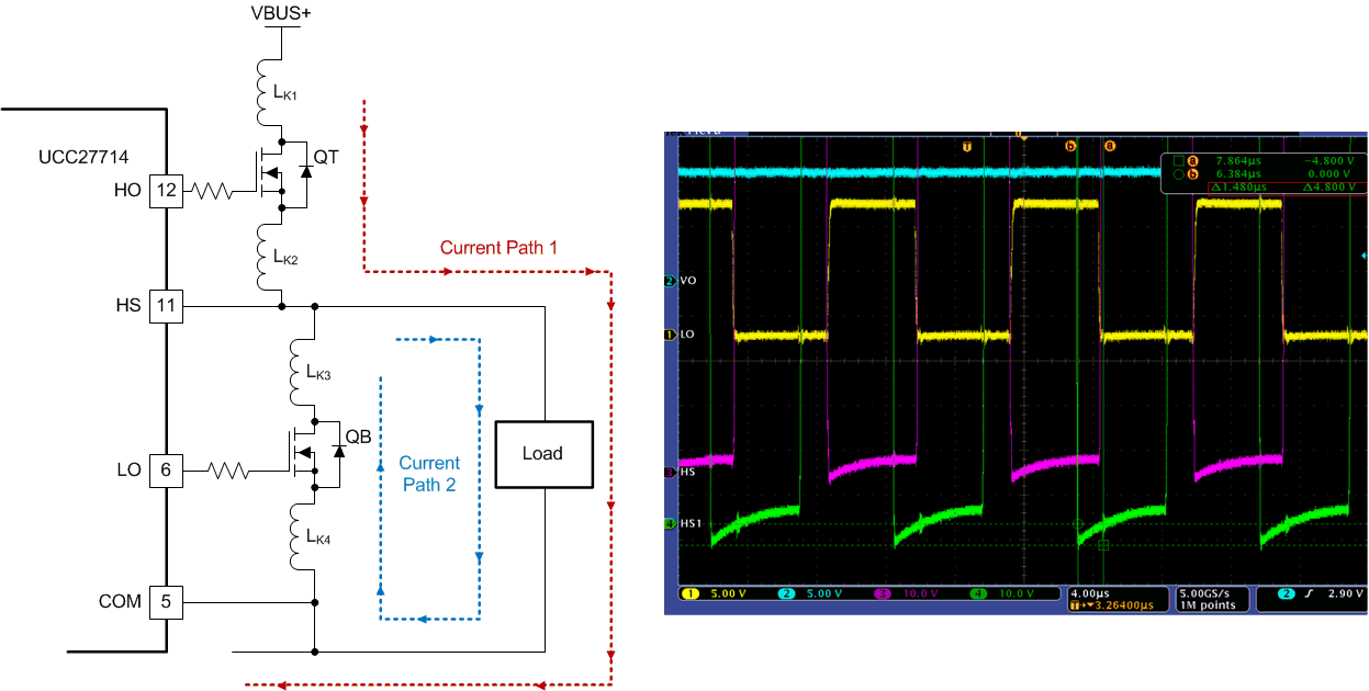 Figure 50. HS Negative Voltage In Half-Bridge Configuration
The level shifter circuit is respect to COM (refer to Functional Block Diagram), the voltage from HB to COM is the supply voltage of level shifter. Under the condition of HS is negative voltage with respect to COM, the voltage of HB-COM is decreased, as shown in Figure 51. There is a minimum operational supply voltage of level shifter, if the supply voltage of level shifter is too low, the level shifter cannot pass through HI signal to HO. The minimum supply voltage of level shifter of UCC27714 is 4 V, so the recommended HS specification is dependent on HB-HS. The specification of recommended HS is –8 V at HB – HS = 12 V.
In general, HS can operate until -8 V when HB – HS = 12 V as the ESD structure in Figure 44 allows a maximum voltage difference of 20 V between both pins. If HB-HS voltage is different, the minimum HS voltage changes accordingly.
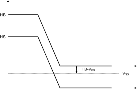 Figure 51. Level Shifter Supply Voltage with Negative HS
NOTE
Logic operational for HS of –8 V to 600 V at HB – HS = 12 V
The capability of a typical UCC27714 device to operate under a negative voltage condition in HS pin is reported in Figure 53. The test method and typical failure mode are shown in Figure 52, where the HO output can be seen to flip from low to high, even while the HI input is held low.
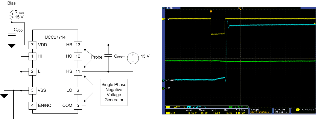 Figure 52. Negative Voltage Test Method and Typical Failure Mode
 Figure 53. Negative Voltage Chart
 Time vs Negative Voltage