SLUS828D December 2008 – October 2017 UCC28019A
PRODUCTION DATA.
- 1 Features
- 2 Applications
- 3 Description
- 4 Revision History
- 5 Pin Configuration and Functions
- 6 Specifications
-
7 Detailed Description
- 7.1 Overview
- 7.2 Functional Block Diagram
- 7.3
Feature Description
- 7.3.1 Soft-Start
- 7.3.2
System Protection
- 7.3.2.1 VCC Undervoltage Lockout (UVLO)
- 7.3.2.2 Input Brown-Out Protection (IBOP)
- 7.3.2.3 Output Overvoltage Protection (OVP)
- 7.3.2.4 Open Loop Protection/Standby (OLP/Standby)
- 7.3.2.5 ISENSE Open-Pin Protection (ISOP)
- 7.3.2.6 Output Undervoltage Detection (UVD) and Enhanced Dynamic Response (EDR)
- 7.3.2.7 Over-Current Protection
- 7.3.2.8 Soft Over Current (SOC)
- 7.3.2.9 Peak Current Limit (PCL)
- 7.3.2.10 Current Sense Resistor, RISENSE
- 7.3.3 Gate Driver
- 7.3.4 Current Loop
- 7.3.5 ISENSE and ICOMP Functions
- 7.3.6 Pulse Width Modulator
- 7.3.7 Control Logic
- 7.3.8 Voltage Loop
- 7.3.9 Output Sensing
- 7.3.10 Voltage Error Amplifier
- 7.3.11 Non-Linear Gain Generation
- 7.4 Device Functional Modes
- 8 Application and Implementation
- 9 Power Supply Recommendations
- 10Layout
- 11Device and Documentation Support
- 12Mechanical, Packaging, and Orderable Information
9 Power Supply Recommendations
9.1 Bias Supply
The UCC28019A operates from an external bias supply. It is recommended that the device be powered from a regulated auxiliary supply.
NOTE
This device is not intended to be used from a bootstrap bias supply. A bootstrap bias supply is fed from the input high voltage through a resistor with sufficient capacitance on VCC to hold up the voltage on VCC until current can be supplied from a bias winding on the boost inductor. For that reason, the minimal hysteresis on VCC would require an unreasonable value of hold-up capacitance.
During normal operation, when the output is regulated, current drawn by the device includes the nominal run current plus the current supplied to the gate of the external boost switch. Decoupling of the bias supply must take switching current into account in order to keep ripple voltage on VCC to a minimum. A ceramic capacitor of 0.1 μF minimum value from VCC to GND with short, wide traces is recommended.
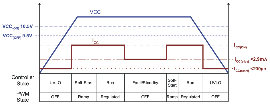
 Figure 33. Device Supply States
The device bias operates in several states. During startup, VCC Under-Voltage Lock-Out (UVLO) sets the minimum operational dc input voltage of the controller. There are two UVLO thresholds. When the UVLO turn-on threshold is exceeded, the PFC controller turns ON. If the VCC voltage falls below the UVLO turn-off threshold, the PFC controller turns off. During UVLO, current drawn by the device is minimal. After the device turns on, Soft Start (SS) is initiated and the boost inductor current is ramped up in a controlled manner to reduce the stress on the external components and avoids output voltage overshoot. During Soft Start and after the output is in regulation, the device draws its normal run current. If any of several fault conditions is encountered or if the device is put in Standby with an external signal, the device draws a reduced standby current.