SGLS121D December 2002 – June 2020 UCC2800-Q1 , UCC2801-Q1 , UCC2802-Q1 , UCC2803-Q1 , UCC2804-Q1 , UCC2805-Q1
PRODUCTION DATA.
- 1 Features
- 2 Applications
- 3 Description
- 4 Revision History
- 5 Description (continued)
- 6 Device Comparison Table
- 7 Pin Configuration and Functions
- 8 Specifications
-
9 Detailed Description
- 9.1 Overview
- 9.2 Functional Block Diagram
- 9.3
Feature Description
- 9.3.1 Detailed Pin Description
- 9.3.2 Undervoltage Lockout (UVLO)
- 9.3.3 Self-Biasing, Active Low Output
- 9.3.4 Reference Voltage
- 9.3.5 Oscillator
- 9.3.6 Synchronization
- 9.3.7 PWM Generator
- 9.3.8 Minimum Off-Time Setting (Dead-Time Control)
- 9.3.9 Leading Edge Blanking
- 9.3.10 Minimum Pulse Width
- 9.3.11 Current Limiting
- 9.3.12 Overcurrent Protection and Full Cycle Restart
- 9.3.13 Soft Start
- 9.3.14 Slope Compensation
- 9.4 Device Functional Modes
- 10Application and Implementation
- 11Power Supply Recommendations
- 12Layout
- 13Device and Documentation Support
- 14Mechanical, Packaging, and Orderable Information
9.3.5 Oscillator
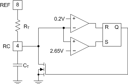
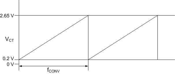
The UCC280x-Q1 oscillator generates a sawtooth waveform on RC. The rise time is set by the time constant of RT and CT. The fall time is set by CT and an internal transistor on-resistance of approximately 130 Ω. During the fall time, the output is OFF and the maximum duty cycle is reduced below 50% or 100%, depending on the part number. Larger timing capacitors increase the discharge time and reduce the maximum duty cycle and frequency.
 Figure 16. Oscillator Equivalent Circuit
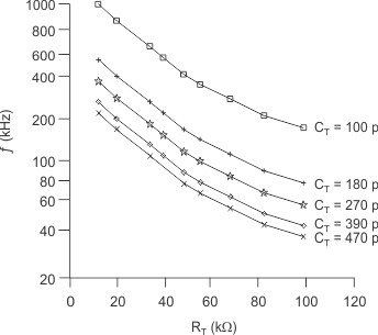
 The oscillator section of the UCC2800-Q1 through UCC2805 BiCMOS devices has few similarities to the UC3842 type — other than single pin programming. It does still use a resistor to the reference voltage and capacitor to ground to program the oscillator frequency up to 1 MHz. Timing component values must be changed because a much lower charging current is desirable for low-power operation. Several characteristics of the oscillator have been optimized for high-speed, noise-immune operation. The oscillator peak-to-peak amplitude has been increased to 2.45 V typical versus 1.7 V on the UC3842 family. The lower oscillator threshold has been dropped to approximately 0.2 V while the upper threshold remains fairly close to the original 2.8 V at approximately
2.65 V.
Discharge current of the timing capacitor has been increased to nearly 20-mA peak as opposed to roughly 8 mA. This can be represented by approximately 130 Ω in series with the discharge switch to ground. A higher current was necessary to achieve brief dead times and high duty cycles with high-frequency operation. Practical applications can use these new ICs to a 1-MHz switching frequency.
 Figure 17. Oscillator Waveform
  Figure 18. Oscillator Frequency vs RT For Several CT