SLUS515G September   2002  – December 2015 UCC28050 , UCC28051 , UCC38050 , UCC38051

PRODUCTION DATA.  

  1. Features
  2. Applications
  3. Description
  4. Revision History
  5. Pin Configuration and Functions
  6. Specifications
    1. 6.1 Absolute Maximum Ratings
    2. 6.2 ESD Ratings
    3. 6.3 Recommended Operating Conditions
    4. 6.4 Thermal Information
    5. 6.5 Electrical Characteristics
    6. 6.6 Typical Characteristics
  7. Detailed Description
    1. 7.1 Overview
    2. 7.2 Functional Block Diagram
    3. 7.3 Feature Description
      1. 7.3.1 UVLO and Reference Block
      2. 7.3.2 Error Amplifier
      3. 7.3.3 Zero Current Detection and Re-Start Timer Blocks
      4. 7.3.4 Enable Block
      5. 7.3.5 Zero Power Block
      6. 7.3.6 Multiplier Block
      7. 7.3.7 Overvoltage Protection (OVP) Block
    4. 7.4 Device Functional Modes
      1. 7.4.1 Transition Mode Control
  8. Application and Implementation
    1. 8.1 Application Information
    2. 8.2 Typical Application
      1. 8.2.1 Design Requirements
      2. 8.2.2 Detailed Design Procedure
        1. 8.2.2.1 Inductor Selection
        2. 8.2.2.2 MOSFET Selection
        3. 8.2.2.3 Diode Selection
        4. 8.2.2.4 Capacitor Selection
        5. 8.2.2.5 Multiplier Set-Up
        6. 8.2.2.6 Sense Resistor Selection
        7. 8.2.2.7 Output Voltage Sense Design
        8. 8.2.2.8 Voltage Loop Design
      3. 8.2.3 Application Curves
  9. Power Supply Recommendations
  10. 10Layout
    1. 10.1 Layout Guidelines
      1. 10.1.1 Bias Current
      2. 10.1.2 Zero Current Detection
    2. 10.2 Layout Example
  11. 11Device and Documentation Support
    1. 11.1 Device Support
      1. 11.1.1 Development Support
    2. 11.2 Related Links
    3. 11.3 Community Resources
    4. 11.4 Trademarks
    5. 11.5 Electrostatic Discharge Caution
    6. 11.6 Glossary
  12. 12Mechanical, Packaging, and Orderable Information

封装选项

请参考 PDF 数据表获取器件具体的封装图。

机械数据 (封装 | 引脚)
  • D|8
  • P|8
散热焊盘机械数据 (封装 | 引脚)
订购信息

10 Layout

10.1 Layout Guidelines

10.1.1 Bias Current

The bias voltage is supplied by a bias winding on the inductor. Select the turns ratio so that sufficient bias voltage can be achieved at low AC line voltage. The bias capacitor must be large enough to maintain sufficient voltage with AC line variations. Connect a 0.1-μF bypass capacitor between the VCC pin and the GND pin as close to the integrated circuit as possible. For wide line variations, a resistor, RB, is necessary to permit clamping action. The bias voltage should also be clamped with an external zener diode to a maximum of 18 V.

10.1.2 Zero Current Detection

The zero current detection activates when the ZCD voltage falls below 1.4 V. The bias winding can provide the necessary voltage. This pin has a clamp at approximately 5 V. Add a current limiting resistor, RZC, to keep the maximum current below 1 mA.

10.2 Layout Example
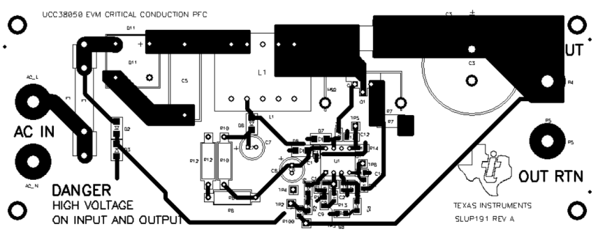
UCC28050 UCC28051 UCC38050 UCC38051 layout_lus515.gif Figure 24. UCC38050 Layout Example
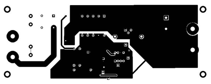
UCC28050 UCC28051 UCC38050 UCC38051 layout4_lus515.gif
Figure 25. UCC38050 Bottom-Layer Layout Example