SLUS515G September 2002 – December 2015 UCC28050 , UCC28051 , UCC38050 , UCC38051
PRODUCTION DATA.
- 1 Features
- 2 Applications
- 3 Description
- 4 Revision History
- 5 Pin Configuration and Functions
- 6 Specifications
- 7 Detailed Description
- 8 Application and Implementation
- 9 Power Supply Recommendations
- 10Layout
- 11Device and Documentation Support
- 12Mechanical, Packaging, and Orderable Information
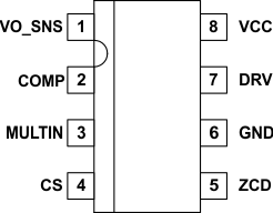
5 Pin Configuration and Functions
D or P Package
8-Pin SOIC or PDIP
Top View

Pin Functions
| PIN | I/O | DESCRIPTION | |
|---|---|---|---|
| NAME | NO. | ||
| COMP | 2 | O | Output of the transconductance error amplifier. Loop compensation components are connected between this pin and ground. The output current capability of this pin is 10-μA under normal conditions, but increases to approximately 1-mA when the differential input is greater than the specified values in the specifications table. This voltage is one of the inputs to the multiplier, with a dynamic input range of 2.5 V to 3.8 V. During zero power or overvoltage conditions, this pin goes below 2.5 V nominal. When it goes below 2.3 V, the zero power comparator is activated, which prevents the gate drive from switching. |
| CS | 4 | I | This pin senses the instantaneous switch current in the boost switch and uses it as the internal ramp for PWM comparator. The internal circuitry filters out switching noise spikes without requiring external components. In addition, an external R-C filter may be required to suppress the noise spikes. An internal clamp on the multiplier output terminates the switching cycle if this pin voltage exceeds 1.7 V. Additional external filtering may be required. CS threshold is approximately equal to: Equation 1. VOFFSET is approximately 75 mV to improve the zero crossing distortion. |
| DRV | 7 | O | The gate drive output for an external boost switch. This output is capable of delivering up to 750-mA peak currents during turn-on and turn-off. An external gate drive resistor may be needed to limit the peak current depending on the VCC voltage being used. Below the UVLO threshold, the output is held low. |
| GND | 6 | – | The chip reference ground. All bypassing elements are connected to ground pin with shortest loops feasible. |
| MULTIN | 3 | I | This pin senses the instantaneous boost regulator input voltage through a voltage divider. The voltage acts as one of the inputs to the internal multiplier. Recommended operating range is 0 V to 2.5 V at high line. |
| VCC | 8 | – | The supply voltage for the chip. This pin should be bypassed with a high-frequency capacitor (greater than 0.1-μF) and tied to GND. The UCC38050 has a wide UVLO hysteresis of approximately 6.3 V that allows use of a lower value supply capacitor on this pin for quicker and easier start-up. The UCC38051 has a narrow UVLO hysteresis with of about 2.8 V, and a start-up voltage of about 12.5 V for applications where the operation of the PFC device must be controlled by a downstream PWM controller. |
| VO_SNS | 1 | I | This pin senses the boost regulator output voltage through a voltage divider. Internally, this pin is the inverting input to the transconductance amplifier (with a nominal value of 2.5 V) and also is input to the OVP comparator. Additionally, pulling this pin below the ENABLE threshold turns off the output switching, ensuring that the gate drive is held off while the boost output is pre-charging, and also ensuring no runaway if the feedback path is open. |
| ZCD | 5 | I | Input for the zero current detect comparator. The boost inductor current is indirectly sensed through the bias winding on the boost inductor. The ZCD pin input goes low when the inductor current reaches zero and that transition is detected. Internal active voltage clamps are provided to prevent this pin from going below ground or too high. If zero current is not detected within 400 μs, a reset timer sets the latch and gate drive. |