ZHCSDH6B December 2014 – March 2015 UCC28063A
PRODUCTION DATA.
- 1 特性
- 2 应用
- 3 说明
- 4 修订历史记录
- 5 说明(继续)
- 6 Pin Configuration and Functions
- 7 Specifications
-
8 Detailed Description
- 8.1 Overview
- 8.2 Functional Block Diagram
- 8.3
Feature Description
- 8.3.1 Principles of Operation
- 8.3.2 Natural Interleaving
- 8.3.3 On-Time Control, Maximum Frequency Limiting, and Restart Timer
- 8.3.4 Distortion Reduction
- 8.3.5 Zero-Current Detection and Valley Switching
- 8.3.6 Phase Management and Light-Load Operation
- 8.3.7 External Disable
- 8.3.8 Improved Error Amplifier
- 8.3.9 Soft Start
- 8.3.10 Brownout Protection
- 8.3.11 Dropout Detection
- 8.3.12 VREF
- 8.3.13 VCC
- 8.3.14 Control of Downstream Converter
- 8.3.15
System Level Protections
- 8.3.15.1 Failsafe OVP - Output Overvoltage Protection
- 8.3.15.2 Overcurrent Protection
- 8.3.15.3 Open-Loop Protection
- 8.3.15.4 VCC Undervoltage Lock-Out (UVLO) Protection
- 8.3.15.5 Phase-Fail Protection
- 8.3.15.6 Thermal Shutdown Protection
- 8.3.15.7 AC-Line Brownout and Dropout Protections
- 8.3.15.8 Fault Logic Diagram
- 8.4 Device Functional Modes
-
9 Applications and Implementation
- 9.1 Application Information
- 9.2
Typical Application
- 9.2.1 Design Requirements
- 9.2.2
Detailed Design Procedure
- 9.2.2.1 Inductor Selection
- 9.2.2.2 ZCD Resistor Selection (RZA, RZB)
- 9.2.2.3 HVSEN
- 9.2.2.4 Output Capacitor Selection
- 9.2.2.5 Selecting (RS) For Peak Current Limiting
- 9.2.2.6 Power Semiconductor Selection (Q1, Q2, D1, D2)
- 9.2.2.7 Brownout Protection
- 9.2.2.8 Converter Timing
- 9.2.2.9 Programming VOUT
- 9.2.2.10 Voltage Loop Compensation
- 9.2.3 Application Curves
- 10Power Supply Recommendations
- 11Layout
- 12器件和文档支持
- 13机械、封装和可订购信息
9 Applications and Implementation
NOTE
Information in the following applications sections is not part of the TI component specification, and TI does not warrant its accuracy or completeness. TI’s customers are responsible for determining suitability of components for their purposes. Customers should validate and test their design implementation to confirm system functionality.
9.1 Application Information
This control IC is generally applicable to the control of AC-DC power supplies which require Active Power Factor Correction off Universal AC line. Applications using this IC will generally meet the Class D equipment input current harmonics standards per EN61000-3-2. This standard applies to equipment with rated Powers higher than 75W. The IC brings two phase interleaved control capability to the Transition Mode Boost and hence will be generally a very good choice for cost optimized applications in the 150W to 800W space, or to even lower powers that wish to exploit the interleaving benefits of reduced filtering component size, lower profile solutions and distributed thermal management.
The UCC28063EVM-723 300-W Interleaved PFC Pre-Regulator User's Guide (SLUU512) describes an EVM design for a 300W Application.
This EVM has an associated Excel file to help automate calculations for its component choices available at SLUC292.
9.2 Typical Application
An example of the UCC28063A PFC controller in a two-phase interleaved, transition-mode PFC pre-regulator is shown in .
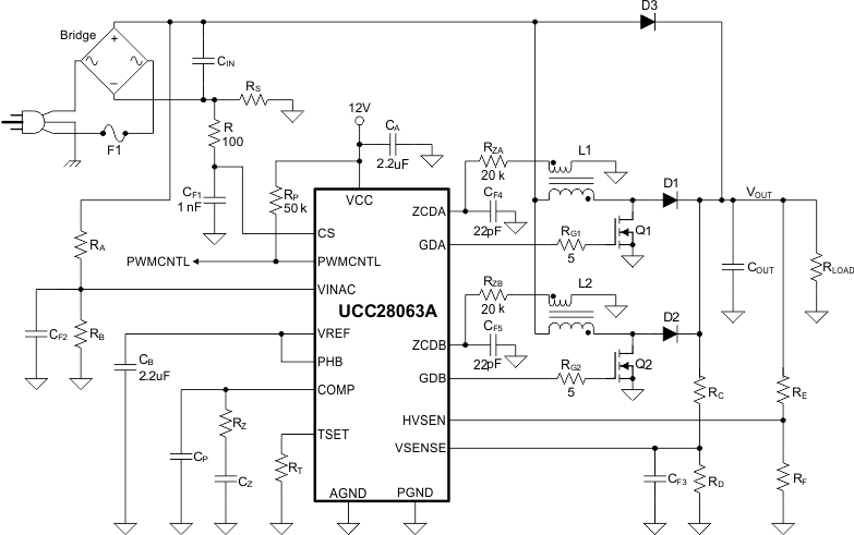 Figure 34. Typical Interleaved Transition-Mode PFC Pre-Regulator
9.2.1 Design Requirements
The specifications for this design were chosen based on the power requirements of a typical 300-W LCD TV. These specifications are shown in Table 2.
Table 2. Design Specifications
| DESIGN PARAMETER | MIN | TYP | MAX | UNIT | |
|---|---|---|---|---|---|
| VIN | RMS input voltage | 85 (VIN_MIN) | 265 (VIN_MAX) | VRMS | |
| VOUT | Output voltage | 390 | V | ||
| fLINE | AC-line frequency | 47 | 63 | Hz | |
| PF | Power factor at maximum load | 0.90 | |||
| POUT | 300 | W | |||
| η | Full-load efficiency | 92% | |||
| fMIN | Minimum switching frequency | 45 | kHz | ||
9.2.2 Detailed Design Procedure
9.2.2.1 Inductor Selection
The boost inductor is selected based on the inductor ripple current requirements at the peak of low line. Selecting the inductor requires calculating the boost converter duty cycle at the peak of low line (DPEAK_LOW_LINE), as shown in Equation 18.

The minimum switching frequency of the converter (fMIN) under low line conditions occurs at the peak of low line and is set between 25 kHz and 50 kHz to avoid audible noise. For this design example, fMIN is set to 45 kHz. For a 2-phase interleaved design, L1 and L2 are determined as shown in Equation 19.

The inductor for this design would have a peak current (ILPEAK) of 5.4 A, as shown in Equation 20, and an RMS current (ILRMS) of 2.2 A, as shown in Equation 21.


This converter uses constant on time (TON) and zero-current detection (ZCD) to set up the converter timing. Auxiliary windings on L1 and L2 detect when the inductor currents are zero. Selecting the turns ratio using Equation 22 ensures that there will be at least 2 V at the peak of high line to reset the ZCD comparator after every switching cycle.
The turns-ratio of each auxiliary winding is:

9.2.2.2 ZCD Resistor Selection (RZA, RZB)
The minimum value of the ZCD resistors is selected based on the internal clamps maximum current ratings of 3 mA, as shown in Equation 23.

In this design the ZCD resistors are set to 20 kΩ, as shown in Equation 24.

9.2.2.3 HVSEN
The HVSEN pin programs the PWMCNTL output of the UCC28063A. The PWMCNTL open-drain output can be used to disable a downstream converter while the PFC output capacitor is charging. PWMCNTL starts high impedance and pulls to ground when HVSEN increases above 2.5 V. Setting the point where PWMCNTL becomes active requires a voltage divider from the boost voltage to the HVSEN pin to ground. Equation 25 to Equation 30 show how to set the PWMCNTL pin to activate when the output voltage is within 90% of its nominal value.

Resistor RE sets up the high side of the voltage divider and programs the hysteresis of the PWMCNTL signal. For this example, RE was selected to provide 99 V of hysteresis, as shown in Equation 26. Three resistors in series were used to meet voltage requirements.

Resistor RF is used to program the PWMCNTL active threshold, as shown in Equation 27.

Select a standard resistor value for RF.

This PWMCNTL output will remain active until a minimum output voltage (VOUT_MIN) is reached, as shown in Equation 29.

According to these resistor values, the FailSafe OVP threshold will be set according to Equation 30

9.2.2.4 Output Capacitor Selection
The output capacitor (COUT) is selected based on holdup requirements, as shown in Equation 31.

Two 100-μF capacitors were used in parallel for the output capacitor.

For this size capacitor, the low-frequency peak-to-peak output voltage ripple (VRIPPLE) is approximately 14 V, as shown in Equation 33:

In addition to holdup requirements, a capacitor must be selected so that it can withstand the low-frequency RMS current (ICOUT_100Hz) and the high-frequency RMS current (ICOUT_HF); see Equation 34 to Equation 36. High-voltage electrolytic capacitors generally have both a low- and a high-frequency RMS current ratings on the product data sheets.


9.2.2.5 Selecting (RS) For Peak Current Limiting
The UCC28063A peak limit comparator senses the total input current and is used to protect the MOSFETs during inrush and over-load conditions. For reliability, the peak current limit (IPEAK) threshold in this design is set for 120% of the nominal maximum current that will be observed during power up, as shown in Equation 37.

A standard 15-mΩ metal-film current-sense resistor will be used for current sensing, as shown in Equation 38. The estimated power loss of the current-sense resistor (PRS) is less than 0.25 W during normal operation, as shown in Equation 39.


The most critical parameter in selecting a current-sense resistor is the surge rating. The resistor needs to withstand a short-circuit current larger than the current required to open the fuse (F1). I2t (ampere-squared- seconds) is a measure of thermal energy resulting from current flow required to melt the fuse, where I2t is equal to RMS current squared times the duration of the current flow in seconds. A 4-A fuse with an I2t of 14 A2s was chosen to protect the design from a short-circuit condition. To ensure the current-sense resistor has high-enough surge protection, a 15-mΩ, 500-mW, metal-strip resistor was chosen for the design. The resistor has a 2.5-W surge rating for 5 seconds. This result translates into 833 A2s and has a high-enough I2t rating to survive a short-circuit before the fuse opens, as described in Equation 40.

9.2.2.6 Power Semiconductor Selection (Q1, Q2, D1, D2)
The selection of Q1, Q2, D1, and D2 are based on the power requirements of the design. Application Note SLUU138, UCC38050 100-W Critical Conduction Power Factor Corrected (PFC) Pre-regulator, explains how to select power semiconductor components for transition-mode PFC pre-regulators.
The MOSFET (Q1, Q2) pulsed-drain maximum current is shown in Equation 41:

The MOSFET (Q1, Q2) RMS current calculation is shown in Equation 42:

To meet the power requirements of the design, IRFB11N50A 500-V MOSFETs were chosen for Q1 and Q2.
The boost diode (D1, D2) RMS current is shown in Equation 43:

To meet the power requirements of the design, MURS360T3, 600-V diodes were chosen for D1 and D2.
9.2.2.7 Brownout Protection
Resistor RA and RB are selected to activate brownout protection at ~75% of the specified minimum-operating input voltage. Resistor RA programs the brownout hysteresis comparator, which is selected to provide 17 V (~12 VRMS) of hysteresis. Calculations for RA and RB are shown in Equation 44 through Equation 47.

To meet voltage requirements, three 2.87-MΩ resistors were used in series for RA.


Select a standard value for RB.

In this design example, brownout becomes active (shuts down PFC) when the input drops below 66 VRMS for longer than 440 ms and deactivates (restarts with a full soft start) when the input reaches 78 VRMS.
9.2.2.8 Converter Timing
The maximum on-time TON depends on fMIN as determined by Equation 48. To ensure proper operation, the timing must be set based on the highest boost inductance (L1MAX) and output power (POUT). In this design example, the boost inductor could be as high as 390 µH. Calculate the timing resistor RT as shown in Equation 49.


This result sets the maximum frequency clamp (fMAX), as shown in Equation 50, which improves efficiency at light load.

9.2.2.9 Programming VOUT
Resistor RC is selected to minimize loading on the power line when the PFC is disabled. Construct resistor RC from two or more resistors in series to meet high-voltage requirements. Resistor RD is then calculated based on RC, the reference voltage, VREF, and the required output voltage, VOUT. Based on the values shown in Equation 51 to Equation 54, the primary output over-voltage protection threshold should be as shown in Equation 55:


Select a standard value for RD.


9.2.2.10 Voltage Loop Compensation
Resistor RZ is sized to attenuate low-frequency ripple to less than 2% of the voltage amplifier output range. This value ensures good power factor and low harmonic distortion on the input current.
The transconductance amplifier small-signal gain is shown in Equation 56:

The voltage-divider feedback gain is shown in Equation 57:

The value of RZ is calculated as shown in Equation 58:

CZ is then set to add 45° phase margin at 1/5th of the line frequency, as shown in Equation 59:

CP is sized to attenuate high-frequency switching noise, as shown in Equation 60:

Standard values should be chosen for RZ, CZ and CP, as shown in Equation 61 to Equation 63.


9.2.3 Application Curves
Refer to UCC28063EVM-723 300-W Interleaved PFC Pre-Regulator EVM User's Guide, SLUU512, for more implementation details and application curves.
9.2.3.1 Input Ripple Current Cancellation with Natural Interleaving
Figure 35 through Figure 37 show the input current (M1= IL1 + IL2), Inductor Ripple Currents (IL1, IL2) versus rectified line voltage. From these graphs, it can be observed that natural interleaving reduces the overall magnitude of input (and output) ripple current caused by the individual inductor current ripples.
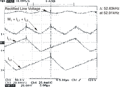 Figure 35. Inductor and Input Ripple Current at 85 VRMS at Peak of Line Voltage
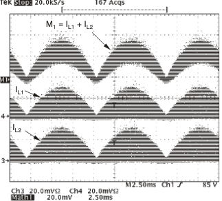 Figure 37. Inductor and Input Ripple Current at VIN = 85 VRMS, POUT = 300 W
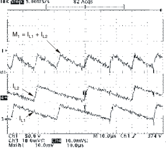 Figure 36. Inductor and Input Ripple Current at 265 VRMS Input at Peak Line Voltage
9.2.3.2 Brownout Protection
The UCC28063A has a brownout protection that shuts down both gate drives (GDA and GDB) when the VINAC pin detects that the RMS input voltage is too low. This EVM was designed to go into a brownout state when the line drops below 64 VRMS. Once the UCC28063A control device has determined that the input is in a brownout condition, a 400-ms timer starts to allow the line to recover before shutting down the gate drivers. After 400 ms of brownout, both gate drivers turn off, as shown in Figure 38.
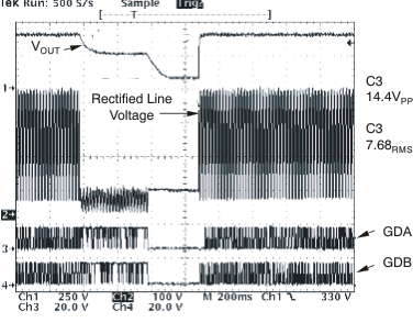 Figure 38. UCC28063A Response to a Line Brownout Event at 265 VRMS