ZHCSIB2B December 2017 – October 2019 UCC28064A
PRODUCTION DATA.
- 1 特性
- 2 应用
- 3 说明
- 4 修订历史记录
- 5 说明 (续)
- 6 Pin Configuration and Functions
- 7 Specifications
-
8 Detailed Description
- 8.1 Overview
- 8.2 Functional Block Diagram
- 8.3
Feature Description
- 8.3.1 Principles of Operation
- 8.3.2 Natural Interleaving
- 8.3.3 On-Time Control, Maximum Frequency Limiting, Restart Timer and Input Voltage Feed-Forward compensation
- 8.3.4 Distortion Reduction
- 8.3.5 Zero-Current Detection and Valley Switching
- 8.3.6 Phase Management and Light-Load Operation
- 8.3.7 Burst Mode Operation
- 8.3.8 External Disable
- 8.3.9 Improved Error Amplifier
- 8.3.10 Soft Start
- 8.3.11 Brownout Protection
- 8.3.12 Line Dropout Detection
- 8.3.13 VREF
- 8.3.14 VCC
- 8.3.15
System Level Protections
- 8.3.15.1 Failsafe OVP - Output Over-voltage Protection
- 8.3.15.2 Overcurrent Protection
- 8.3.15.3 Open-Loop Protection
- 8.3.15.4 VCC Undervoltage Lock-Out (UVLO) Protection
- 8.3.15.5 Phase-Fail Protection
- 8.3.15.6 CS - Open, TSET - Open and Short Protection
- 8.3.15.7 Thermal Shutdown Protection
- 8.3.15.8 Fault Logic Diagram
- 8.4 Device Functional Modes
-
9 Application and Implementation
- 9.1 Application Information
- 9.2
Typical Application
- 9.2.1 Design Requirements
- 9.2.2
Detailed Design Procedure
- 9.2.2.1 Custom Design With WEBENCH® Tools
- 9.2.2.2 Inductor Selection
- 9.2.2.3 ZCD Resistor Selection RZA, RZB
- 9.2.2.4 HVSEN
- 9.2.2.5 Output Capacitor Selection
- 9.2.2.6 Selecting RS For Peak Current Limiting
- 9.2.2.7 Power Semiconductor Selection (Q1, Q2, D1, D2)
- 9.2.2.8 Brownout Protection
- 9.2.2.9 Converter Timing
- 9.2.2.10 Programming VOUT
- 9.2.2.11 Voltage Loop Compensation
- 9.2.3 Application Curves
- 10Power Supply Recommendations
- 11Layout
- 12Package Option Addendum
- 13器件和文档支持
- 14机械、封装和可订购信息
8.3.6 Phase Management and Light-Load Operation
It is challenging to maintain high efficiency under all loading conditions. When operating in light-load, switching losses may dominate over conduction losses and the efficiency may be improved if one phase is turned off. Turning off a phase at light load is especially valuable for meeting light-load efficiency standards. This is a major benefit of interleaved PFC and it is especially valuable for meeting 80+ design requirements.
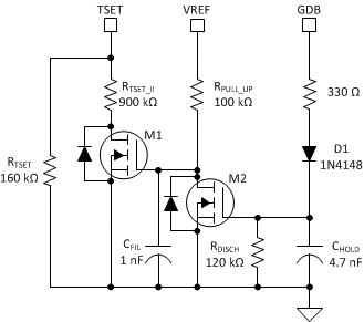
In order to ensure smooth operation when removing or adding a phase, some additional considerations are required. When the number of phases operating is changed from 2 to 1 the overall switching frequency is reduced by a factor of 2. If everything else is held constant this will also reduce the energy delivered to the load by a factor of 2. In order to maintain the same power delivery to the output, it is necessary to increase the on-time when performing such a transition. A similar situation exists when a phase is added. In other words, when going from 1 phase to 2 phases, the on-time should decrease in order to have smooth continuous power delivery. If everything is ideal, the amount by which the system has to increase/decrease the on-time is a factor of 2. Since 1 phase needs to deliver twice the energy as each phase when both phases are operating, doubling the on-time would seem to make the most sense (or cutting it in half if going from 1 phase to 2 phases). While this works well in many cases there are real world examples where this fails to provide a sufficiently smooth phase shedding/adding operation. In order to resolve this conflict the circuit in Figure 20 can be utilized to program a custom on-time for both 1 phase and 2 phase operation. The circuit operates by monitoring the gate drive of phase 2 (GDB). When this signal is active the resistor RTSET configures the on-time. When the gate drive is absent the on-time is configured by the parallel combination of RTSET and RTSET_II. The capacitors CFIL and CHOLD can be adjusted to set up custom delays in the phase shedding/adding process.
 Figure 20. External circuit for Enhanced Phase Shedding
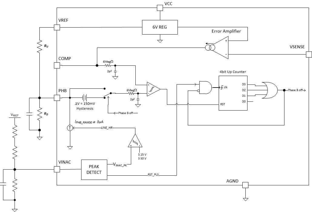
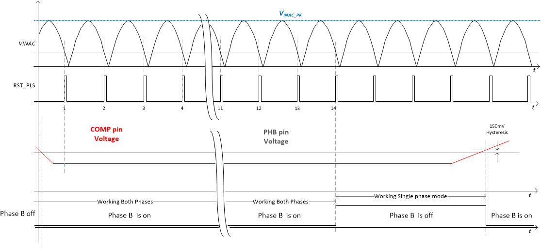
 In the case where the 2x factor is sufficient, the UCC28064A can manage this phase shedding/adding process without the need of the circuit in Figure 20.The PHB input can be used to set the load value when the UCC28064A has to operate in single-phase mode. The UCC28064A internally compares the voltage fed to PHB pin with the COMP pin voltage. If COMP is below PHB channel B will stop switching and the channel A on-time will automatically double to compensate the missing power from channel B. When operating in single phase mode in order to avoid risk of inductor saturation an internal clamp ensures the on time never can exceed the maximum on-time you will have when operating in dual phase mode. The device will resume dual-phase mode when the COMP pin voltage exceeds PHB voltage plus the PHB hysteresis. In order to avoid voltage ripple on the COMP pin causing the system to oscillate between one and two phases a time delay filter is present. In order to change from normal operation to single phase mode the COMP voltage should stay below PHB pin voltage for 14 line half cycles. The filter does not apply for the opposite transition. When the COMP pin voltage exceeds PHB pin voltage plus the hysteresis, channel B is immediately turned on and the channel A on-time is halved.
At start up, the output voltage can be very close to the peak line voltage. The inductor current value during the off time will decrease very slowly and it is possible systems will operate in CCM for a few switching cycles. In order to avoid high current, during soft start, the system is forced to work with both phases on even if the COMP pin voltage is below PHB pin voltage. In two phase mode the on-time of each phase is one half of the on time of phase A when Phase B is off so this mitigates the risk of high CCM currents.
 Figure 21. Phase Management Block Diagram
  Figure 22. Phase Management Time Diagram
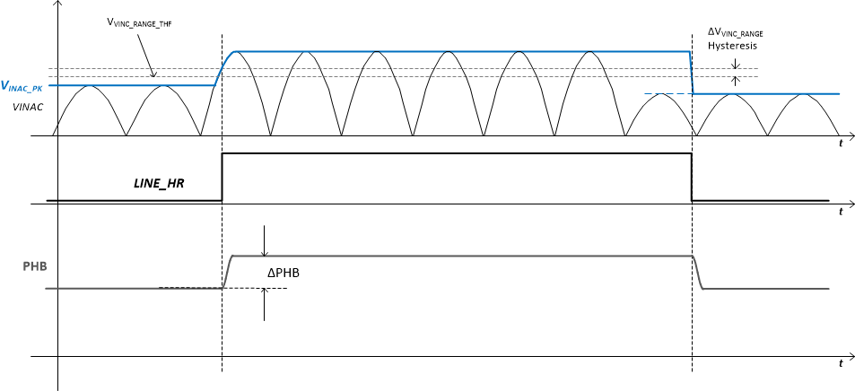
 The voltage on the PHB pin can be set using a simple resistor divider connected to the VREF pin. Another important feature, that allows optimization of phase management is that it is possible to set different thresholds wether the PFC input voltage is in the range of 90 to 132 VRMS (US mains) or in the range of 180 to 265 VRMS (European mains). If the peak voltage sensed by the VINAC pin exceeds 3.5V the converter assumes that the input voltage is in the range of 180 to 265 VRMS and starts sourcing from PHB a small current (3µA typically) that increases the voltage on PHB pin.
 Figure 23. Change Phase Management Thresholds
 Use Equation 5 and Equation 6 to calculate PHB thresholds.


The load value at which the system moves between single phase and dual phase modes of operation is part of the system specification. The formulas to calculate resistor divider resistance values that allows us to get the desired thresholds are reported below.


where
- RD is the lower resistor of the resistor divider that provides voltage to PHB pin that is supplied by VREF
- RU is the upper resistor of the resistor divider.

PHB thresholds are selected by the user according to the load value where they want to turn off Phase B. So assuming we want to turn off Phase B when the load goes below POUT_PHB we can calculate the threshold using equation (10). We can use the same equation in order to calculate the two thresholds VPHB_HR and VPHB_LR once provided the two different load values, for US range and EU range where Phase B has to be turned off. Of course main EU range PHB_OFF load value has to be greater than main US range PHB_OFF load value. A reasonable range of load values is from 20% to 30% of converter rated power.

When the COMP voltage goes below the burst mode threshold the device is forced to work in single phase mode so if the COMP pin voltage drops below the burst threshold it is possible that the time delay filtering is not respected. Moreover it is recommended that PHB pin voltage is at least 600mV higher than BRST pin voltage.