SGLS245E May 2020 – May 2020 UCC2813-0-Q1 , UCC2813-1-Q1 , UCC2813-2-Q1 , UCC2813-3-Q1 , UCC2813-4-Q1 , UCC2813-5-Q1
PRODUCTION DATA.
- 1 Features
- 2 Applications
- 3 Description
- 4 Revision History
- 5 Device Comparison Table
- 6 Pin Configuration and Functions
- 7 Specifications
-
8 Detailed Description
- 8.1 Overview
- 8.2 Functional Block Diagram
- 8.3
Feature Description
- 8.3.1 Detailed Pin Descriptions
- 8.3.2 Undervoltage Lockout (UVLO)
- 8.3.3 Self-Biasing, Active Low Output
- 8.3.4 Reference Voltage
- 8.3.5 Oscillator
- 8.3.6 Synchronization
- 8.3.7 PWM Generator
- 8.3.8 Minimum Off-Time Adjustment (Dead-Time Control)
- 8.3.9 Leading Edge Blanking
- 8.3.10 Minimum Pulse Width
- 8.3.11 Current Limiting
- 8.3.12 Overcurrent Protection and Full-Cycle Restart
- 8.3.13 Soft Start
- 8.3.14 Slope Compensation
- 8.4 Device Functional Modes
-
9 Application and Implementation
- 9.1 Application Information
- 9.2
Typical Application
- 9.2.1 Design Requirements
- 9.2.2
Detailed Design Procedure
- 9.2.2.1 Bulk Capacitor Calculation
- 9.2.2.2 Transformer Design
- 9.2.2.3 MOSFET and Output Diode Selection
- 9.2.2.4 Output Capacitor Calculation
- 9.2.2.5 Current Sensing Network
- 9.2.2.6 Gate Drive Resistor
- 9.2.2.7 REF Bypass Capacitor
- 9.2.2.8 RT and CT
- 9.2.2.9 Start-Up Circuit
- 9.2.2.10 Voltage Feedback Compensation Procedure
- 9.2.3 Application Curves
- 10Power Supply Recommendations
- 11Layout
- 12Device and Documentation Support
- 13Mechanical, Packaging, and Orderable Information
8.3.8 Minimum Off-Time Adjustment (Dead-Time Control)
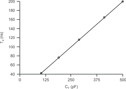
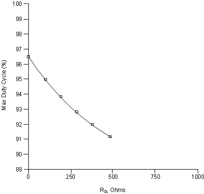
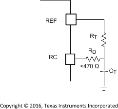
Dead time is the term used to describe the ensured OFF time of the PWM output during each oscillator cycle. It is used to ensure that even at maximum duty cycle, there is enough time to reset the magnetic circuit elements, and prevent saturation. The dead time of the UCC2813-x-Q1 PWM family is determined by the internal 130-Ω discharge impedance and the timing capacitor value. Larger capacitance values extend the dead time whereas smaller values results in higher maximum duty cycles for the same operating frequency. A curve for dead time versus timing capacitor values is provided in Figure 20. Further increasing the dead time is possible by adding a low-value resistor between the RC pin and the timing components, as shown in Figure 21. The dead time increases with increasing discharge resistor value to about 470 Ω as indicated from the curve in Figure 22. Higher resistances must be avoided as they can decrease the dead time and reduce the oscillator peak-to-peak amplitude. Sinking too much current (1 mA) by reducing RT will freeze the oscillator OFF by preventing discharge to the lower comparator threshold voltage of 0.2 V. Adding this discharge control resistor has several impacts on the oscillator programming. First, it introduces a DC offset to the capacitor during the discharge interval – but not the charging interval of the timing cycle, thus lowering the usable peak-to-peak timing capacitor amplitude. Because of the reduced peak-to-peak amplitude, the exact value of CT may require adjustment to obtain the correct oscillator frequency. One alternative is keep the same value timing capacitor and adjust both the timing and discharge resistor values because these are readily available in finer numerical increments.
 Figure 20. Minimum Dead Time vs CT
| RT = 20 kΩ |
 Figure 21. Circuit to Produce Controlled Maximum Duty Cycle