SGLS245E May 2020 – May 2020 UCC2813-0-Q1 , UCC2813-1-Q1 , UCC2813-2-Q1 , UCC2813-3-Q1 , UCC2813-4-Q1 , UCC2813-5-Q1
PRODUCTION DATA.
- 1 Features
- 2 Applications
- 3 Description
- 4 Revision History
- 5 Device Comparison Table
- 6 Pin Configuration and Functions
- 7 Specifications
-
8 Detailed Description
- 8.1 Overview
- 8.2 Functional Block Diagram
- 8.3
Feature Description
- 8.3.1 Detailed Pin Descriptions
- 8.3.2 Undervoltage Lockout (UVLO)
- 8.3.3 Self-Biasing, Active Low Output
- 8.3.4 Reference Voltage
- 8.3.5 Oscillator
- 8.3.6 Synchronization
- 8.3.7 PWM Generator
- 8.3.8 Minimum Off-Time Adjustment (Dead-Time Control)
- 8.3.9 Leading Edge Blanking
- 8.3.10 Minimum Pulse Width
- 8.3.11 Current Limiting
- 8.3.12 Overcurrent Protection and Full-Cycle Restart
- 8.3.13 Soft Start
- 8.3.14 Slope Compensation
- 8.4 Device Functional Modes
-
9 Application and Implementation
- 9.1 Application Information
- 9.2
Typical Application
- 9.2.1 Design Requirements
- 9.2.2
Detailed Design Procedure
- 9.2.2.1 Bulk Capacitor Calculation
- 9.2.2.2 Transformer Design
- 9.2.2.3 MOSFET and Output Diode Selection
- 9.2.2.4 Output Capacitor Calculation
- 9.2.2.5 Current Sensing Network
- 9.2.2.6 Gate Drive Resistor
- 9.2.2.7 REF Bypass Capacitor
- 9.2.2.8 RT and CT
- 9.2.2.9 Start-Up Circuit
- 9.2.2.10 Voltage Feedback Compensation Procedure
- 9.2.3 Application Curves
- 10Power Supply Recommendations
- 11Layout
- 12Device and Documentation Support
- 13Mechanical, Packaging, and Orderable Information
8.3.10 Minimum Pulse Width
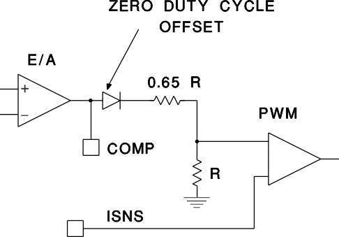
The PWM comparator has two inputs; one is from the current sense input, the other input is the attenuated error-amplifier output (COMP) that has a diode and two resistors in series to ground. The diode in this network is used to ensure that zero duty-cycle can be reached. Whenever the E/A output falls below a diode forward voltage drop, no current flows in the resistor divider and the PWM input goes to zero, resulting in zero pulse width.
Under certain conditions, the leading-edge-blanking circuitry can lead to an output pulse of minimum width equal to the blanking interval. This occurs when the COMP is slightly higher than a diode forward voltage drop of about 0.5 V, such that the attenuated COMP input to the PWM comparator allows an output pulse to start. If the attenuated COMP level commands a peak current whose pulse width would fall within the leading-edge-blanking interval, the output will remain ON until the blanking interval is finished and the peak current will be higher than desired by the COMP level. The usual result is that the converter output voltage rises, increasing the error, and COMP is driven lower than the diode drop which then produces zero pulse width. Cycle-skipping may result as the output voltage rises and falls around this minimum pulse-width condition.
 Figure 25. Zero Duty-Cycle Offset