SGLS245E May 2020 – May 2020 UCC2813-0-Q1 , UCC2813-1-Q1 , UCC2813-2-Q1 , UCC2813-3-Q1 , UCC2813-4-Q1 , UCC2813-5-Q1
PRODUCTION DATA.
- 1 Features
- 2 Applications
- 3 Description
- 4 Revision History
- 5 Device Comparison Table
- 6 Pin Configuration and Functions
- 7 Specifications
-
8 Detailed Description
- 8.1 Overview
- 8.2 Functional Block Diagram
- 8.3
Feature Description
- 8.3.1 Detailed Pin Descriptions
- 8.3.2 Undervoltage Lockout (UVLO)
- 8.3.3 Self-Biasing, Active Low Output
- 8.3.4 Reference Voltage
- 8.3.5 Oscillator
- 8.3.6 Synchronization
- 8.3.7 PWM Generator
- 8.3.8 Minimum Off-Time Adjustment (Dead-Time Control)
- 8.3.9 Leading Edge Blanking
- 8.3.10 Minimum Pulse Width
- 8.3.11 Current Limiting
- 8.3.12 Overcurrent Protection and Full-Cycle Restart
- 8.3.13 Soft Start
- 8.3.14 Slope Compensation
- 8.4 Device Functional Modes
-
9 Application and Implementation
- 9.1 Application Information
- 9.2
Typical Application
- 9.2.1 Design Requirements
- 9.2.2
Detailed Design Procedure
- 9.2.2.1 Bulk Capacitor Calculation
- 9.2.2.2 Transformer Design
- 9.2.2.3 MOSFET and Output Diode Selection
- 9.2.2.4 Output Capacitor Calculation
- 9.2.2.5 Current Sensing Network
- 9.2.2.6 Gate Drive Resistor
- 9.2.2.7 REF Bypass Capacitor
- 9.2.2.8 RT and CT
- 9.2.2.9 Start-Up Circuit
- 9.2.2.10 Voltage Feedback Compensation Procedure
- 9.2.3 Application Curves
- 10Power Supply Recommendations
- 11Layout
- 12Device and Documentation Support
- 13Mechanical, Packaging, and Orderable Information
8.3.2 Undervoltage Lockout (UVLO)
The UCC2813-x-Q1 devices feature undervoltage lockout protection circuits for controlled operation during power-up and power-down sequences. Both the supply voltage (VVCC) and the reference voltage (VREF) are monitored by the UVLO circuitry. During UVLO, an active-low, self-biasing totem-pole output structure is also incorporated for enhanced power switch protection.
Undervoltage lockout thresholds for the UCC2813-[2,3,4,5]-Q1 devices are different from the previous generation of UCx84[2,3,4,5]-Q1 PWM controllers. The thresholds are optimized for two groups of applications: off-line power supplies and DC-DC converters. See Table 1 for the specific thresholds for each device.
Table 1. UVLO Level Comparison Table
| DEVICE | VON (V) | VOFF (V) |
|---|---|---|
| UCC2813-0-Q1 | 7.2 | 6.9 |
| UCC2813-1-Q1 | 9.4 | 7.4 |
| UCC2813-[2,4]-Q1 | 12.5 | 8.3 |
| UCC2813-[3,5]-Q1 | 4.1 | 3.6 |
The UCC2813-[2,4]-Q1 feature typical UVLO thresholds of 12.5 V for turnon and 8.3 V for turnoff, providing 4.3 V of hysteresis.
For low voltage inputs, which include battery and 5-V applications, the UCC2813-[3,5]-Q1 turn on at 4.1 V and turn off at 3.6 V with 0.5 V of hysteresis.
The UCC2813-[0,1]-Q1 have UVLO thresholds optimized for automotive and battery applications.
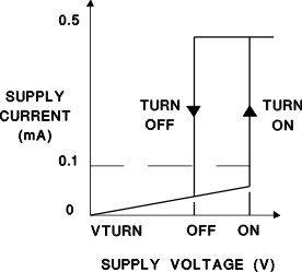
During UVLO, the device draws approximately 100 µA of supply current. Once VCC crosses the turnon threshold, the device supply current increases typically to about 500 µA, over an order of magnitude lower than bipolar counterparts. Figure 11 indicates the supply current behavior at the relative UVLO turnon and turnoff thresholds, not including average OUT current.
 Figure 11. Device Supply Current at UVLO