SLUSA29D April 2010 – August 2015 UCC28250
PRODUCTION DATA.
- 1 Features
- 2 Applications
- 3 Description
- 4 Revision History
- 5 Pin Configuration and Functions
- 6 Specifications
-
7 Detailed Description
- 7.1 Overview
- 7.2 Functional Block Diagram
- 7.3
Feature Description
- 7.3.1 VDD (5/12)
- 7.3.2 VREF (Reference Generator) (20/7)
- 7.3.3 EN (Enable Pin) (18/5)
- 7.3.4 RT (Oscillator Frequency Set and Synchronization) (15/2)
- 7.3.5 SP (Synchronous Rectifier Turnoff to Primary Output Turnon Dead Time Programming) (13/19)
- 7.3.6 PS (Primary Output Turnoff to Synchronous Rectifier Turnon Dead Time Programming) (11/18)
- 7.3.7 RAMP/CS (PWM Ramp Input or Current Sense Input) (16/3)
- 7.3.8 REF/EA+ (1/8)
- 7.3.9 FB/EA- (2/9)
- 7.3.10 COMP (3/10)
- 7.3.11 VSENSE (14/1)
- 7.3.12 SS (Soft Start Programming Pin) (13/20)
- 7.3.13 ILIM (Current Limit for Cycle-By-Cycle Overcurrent Protection) (17/4)
- 7.3.14 HICC (10/17)
- 7.3.15 OVP/OTP (19/6)
- 7.3.16 OUTA (9/16) and OUTB (8/15)
- 7.3.17 SRA (7/14) and SRB (6/13)
- 7.3.18 GND (4/11)
- 7.4 Device Functional Modes
-
8 Applications and Implementation
- 8.1 Application Information
- 8.2
Typical Applications
- 8.2.1
Design Example
- 8.2.1.1 Design Requirements
- 8.2.1.2
Detailed Design Procedure
- 8.2.1.2.1 Step 1, Power Stage Design
- 8.2.1.2.2 Step 2, Feedback Loop Design
- 8.2.1.2.3 Step 3, Programming the Device
- 8.2.1.2.4 Step 3-3, Determine Soft-Start Capacitance
- 8.2.1.2.5 Step 3-4, Determine Dead-Time Resistance
- 8.2.1.2.6 Step 3-5, Determine OCP Hiccup Off-Time Capacitance
- 8.2.1.2.7 Step 3-6, Determine Primary-Side OVP Resistance
- 8.2.1.2.8 Step 3-7, Select Capacitance for VDD and VREF
- 8.2.1.3 Application Curves
- 8.2.2 Secondary-Side Half-Bridge Controller with Synchronous Rectification
- 8.2.1
Design Example
- 9 Power Supply Recommendations
- 10Layout
- 11Device and Documentation Support
- 12Mechanical, Packaging, and Orderable Information
封装选项
机械数据 (封装 | 引脚)
散热焊盘机械数据 (封装 | 引脚)
- RGP|20
订购信息
7 Detailed Description
7.1 Overview
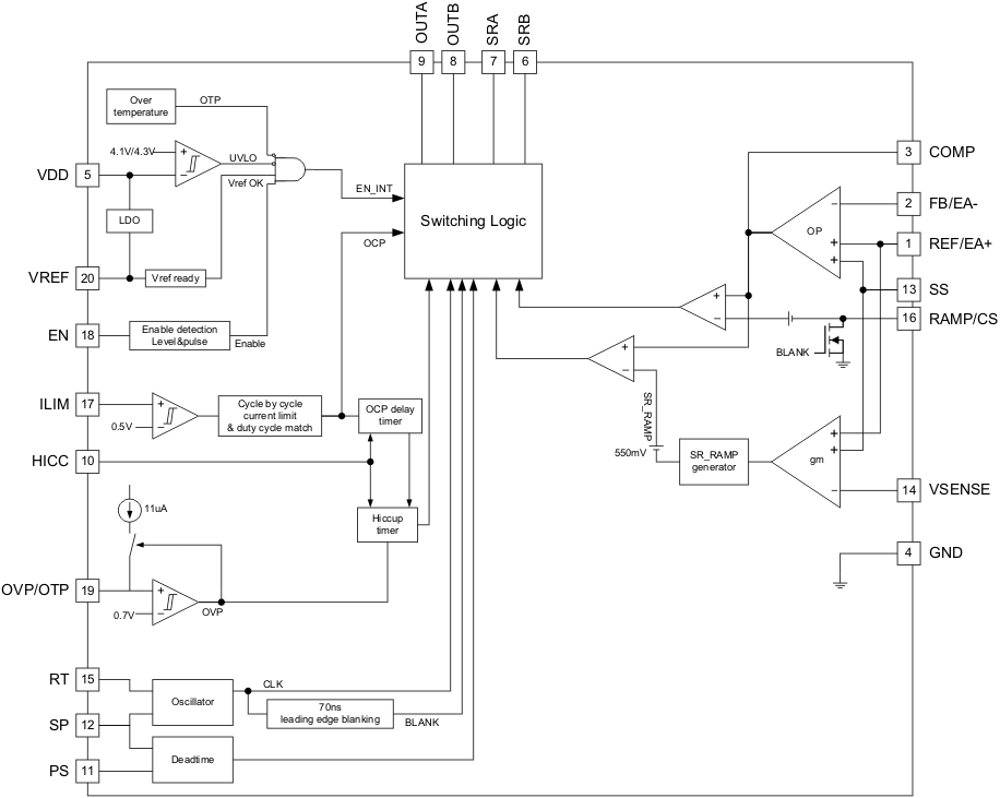
The UCC28250 is a high-performance PWM controller with advanced synchronous rectifier outputs and is ideally suited for regulated half-bridge, full-bridge and push-pull converters. A dedicated internal prebiased start-up control loop working in conjunction with a primary-side voltage loop achieves prebiased start-up for either primary-side or secondary-side control applications. The UCC28250 architecture allows either voltage mode or current mode control.
Input voltage feedforward can be implemented, allowing PWM ramp generator to improve the converter line transient response. Advanced cycle-by-cycle current limit achieves volt-second balancing even during fault conditions. The hiccup timer helps the system to stay within a safe operation range under over load conditions. With a multifunction OVP/OTP pin, combinations of input voltage protection, output voltage protection and overtemperature protection can be implemented. The UCC28250 allows individual programming of dead time between primary-side switch and secondary-side SRs, to allow optimal power stage design. Dead time can also be reduced to zero, and this allows optimal system configuration considering the delays on the gate driver stage. The UCC28250 also provides complete system level protection functions, including UVLO, thermal shut down and overvoltage, overcurrent protection.
7.2 Functional Block Diagram
7.3 Feature Description
7.3.1 VDD (5/12)
The UCC28250 can be powered up by a wide supply range from 4.3 V (UVLO rising typical) to 20 V (absolute maximum), making it suitable for primary-side control or secondary-side control. When the voltage at the VDD pin is lower than 4.1 V (typical), the controller is in stand-by mode and consumes 150 µA (typical) at 3.6 V VDD. In stand-by mode, VREF continues to be regulated to 3.3 V or follows VDD if VDD is lower than 3.3 V. Refer to the VREF description VREF (Reference Generator) (20/7) for more detailed information. A minimum 1-µF bypass capacitor is required from VDD to ground. Keep the bypass capacitor as close to the device as possible.
7.3.2 VREF (Reference Generator) (20/7)
The VREF pin is regulated at 3.3 V. An external ceramic capacitor must be placed as close as possible to the VREF and GND pins for noise filtering and to provide compensation to the regulator. The capacitance range must be limited from 0.5 µF to 2 µF for stability. This reference is used to power the controller’s internal circuits, and can also be used to bias an opto-coupler transistor, an external house-keeping microcontroller, or other peripheral circuits. This reference can also be used to generate the reference for an external error amplifier. This regulator output is internally current limited to 25 mA (typical).
7.3.3 EN (Enable Pin) (18/5)
The following conditions must be met before the controller allows start-up:
- VDD voltage is above the rising UVLO threshold 4.3 V (typical).
- The 3.3-V reference voltage output at the VREF pin is available and above 2.4 V (typical).
- Junction temperature is below the thermal shutdown threshold 130°C (minimum).
- The voltage at OVP is below 0.7 V (typical).
If all these conditions are met, the signal driving the EN pin is able to initiate the soft start process. When the device is enabled, the 27-µA internal charging current at the SS pin is turned on and begins to charge the soft-start capacitor. The EN pin can accept both level-enable and pulse-enable signals.
For level-enable, the voltage level on the EN pin must be continuously higher than 2.25 V to allow continuous operation. When the EN pin falls below 2.25 V, the device is disabled (see Figure 21).
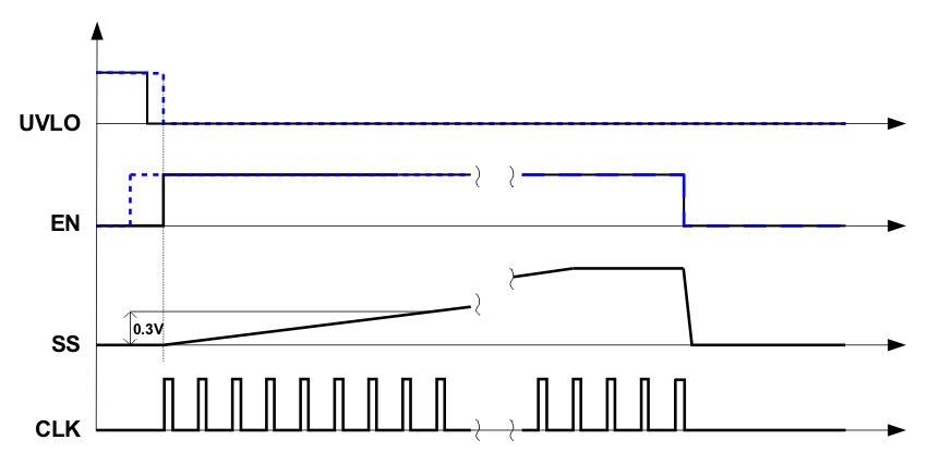 Figure 21. Level Enable at EN pin
A pulse signal may also be applied to the EN pin. Pulse-enable operation is shown on Figure 22. As long as the EN falling edge happens before the SS voltage reaches 0.3 V, the enable signal at EN pin is considered as a pulse. In this case, the next rising edge at EN pin disables the controller. As long as the falling edge of the first pulse at EN pin happens after SS rises to 0.3 V, the UCC28250 interprets the pulse enable as a level enable, and an external solution as shown on Figure 23 (a) can be used to reduce the pulse width. In this circuit, R2 is used to limit the current (especially the negative current) through the internal ESD cell. Figure 23 (b) illustrates the waveforms based on this solution. To prevent false trigger by noises, the pulse at the EN pin must be at least 2.25 V (minimum) high and 3 µs wide to be considered valid.
Choose the R1, R2, and C values based on the following equations:
Choose R2 based on the current limit requirement from the device.

Choose R1 arbitrarily but much smaller than R2 and choose C1 according to the time constant requirement to generate longer than 3-µs pulse.

In the case that the UCC28250 is enabled with a level EN signal and the SS is discharged internally when the OCP is triggered, pulling the EN pin down before SS rises to 0.3 V cannot disable the part because the controller interprets it to be a pulse enable. In this case, the next rising edge at the EN pin disables the controller. If the designer wants to disable UCC28250 with a level signal during an over current condition, the recommended solution is to pull down the SS pin rather than the EN pin. If the enable function is not used, pull the EN pin to the VREF pin.
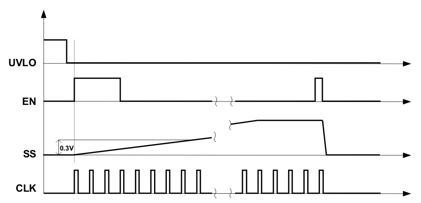 Figure 22. Pulse Enable at EN Pin
 Figure 23. An External Solution to Generate Enable Pulses for Pulse Enable
7.3.4 RT (Oscillator Frequency Set and Synchronization) (15/2)
The UCC28250 oscillator frequency is set by an external resistor connected between the RT pin and ground. Switching frequency selection is a trade-off between efficiency and component size. Based on the selected switching frequency, the programming resistor value can be calculated as:

In this equation, fSW is the switching frequency and TD(sp) is the dead time between synchronous rectifier turnoff to primary switch turnon. TD(sp) is set by an external resistor between the SP pin and ground (refer to SP (Synchronous Rectifier Turnoff to Primary Output Turnon Dead Time Programming) (13/19)).
Each output (OUTA, OUTB, SRA, SRB) switches at half the oscillator frequency (fSW = ½ x fOSC). Figure 24 shows the relationship between RT and fOSC at certain TD(sp) and can be used to program oscillator frequency accordingly.
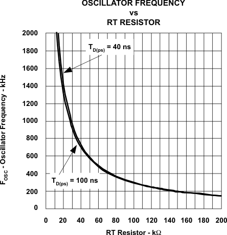 Figure 24. Oscillator Frequency FOSC vs External Resistance of RT at TD(ps) = 40 ns and 100 ns
The UCC28250 can be synchronized to an external clock by applying an external clock source to the RT pin. Synchronization helps with parallel operation and/or preventing beat frequency noise. The UCC28250 synchronizes its internal oscillator to an external frequency source ranging from 170 kHz to 2.3 MHz, which is equivalent to an 85-kHz to 1.15-MHz switching frequency. The internal oscillator frequency is clamped to 170 kHz during synchronization if the external source frequency drops below 170 kHz.
The UCC28250 aligns the turnon of primary outputs OUTA and OUTB to the falling edge of the synchronizing signal, as shown in Figure 25. If the frequency source is from the gate outputs of another half bridge controller, interleaving can be achieved. The interleaving angle is determined by the frequency source’s duty cycle. When a 50% duty cycle is applied, optimal interleaving is achieved, and EMI filters can be minimized.
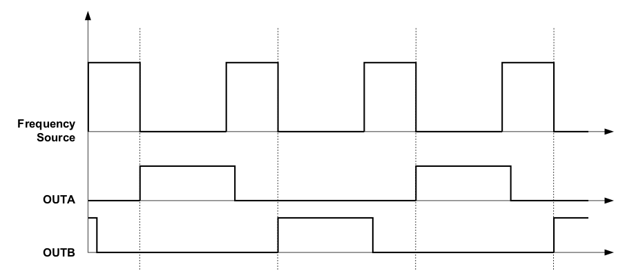 Figure 25. Timing Diagram for Synchronization
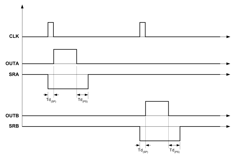 Figure 26. UCC28250 Outputs Timing Waveforms
7.3.5 SP (Synchronous Rectifier Turnoff to Primary Output Turnon Dead Time Programming) (13/19)
The dead time TD(sp) between synchronous rectifier turnoff to primary output turnon is programmed by an external resistor, RSP, connected between the SP pin and ground. The value of RSP can be determined by Figure 27. Zero dead time can be achieved by tying the SP pin to VREF. The falling edge of synchronous rectifier SRA/SRB is aligned with the raising edge of the primary output OUTA/OUTB.
NOTE
The minimum value for RPS/RSP is 5 kΩ and the maximum value is 250 kΩ.
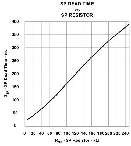 Figure 27. Dead Time TD(sp) vs. External Resistor RSP at SP Pin
7.3.6 PS (Primary Output Turnoff to Synchronous Rectifier Turnon Dead Time Programming) (11/18)
The dead time TD(ps) between primary output turnoff to synchronous rectifier turnon is set by external resistor, RPS, connected between PS pin and ground. The value of is RPS is defined by Figure 28. Zero dead time can be achieved by tying the SP pin to VREF.
NOTE
The minimum value for RPS/RSP is 5 kΩ and the maximum value is 250 kΩ.
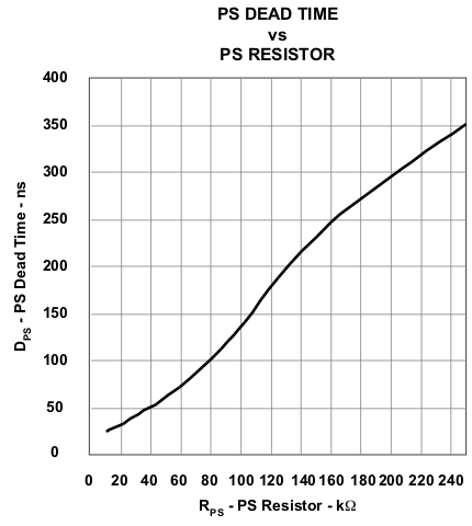 Figure 28. Dead Time TD(ps) vs. External Resistor RPS at PS Pin
7.3.7 RAMP/CS (PWM Ramp Input or Current Sense Input) (16/3)
The UCC28250 can be controlled using either voltage mode or current mode. RAMP/CS is a multi-function pin used either to generate the ramp signal for voltage mode control or to sense current for current mode control.The following sections describe the RAMP/CS functionality for voltage mode and current mode control.
7.3.7.1 RAMP: Voltage Mode Control With Feed-Forward Operation
For voltage mode control, a resistor RCS and a capacitor CCS must be connected to the RAMP/CS pin as shown in Figure 29. The internal pulldown switch has approximately 40-Ω on-resistance. The RAMP/CS pin is clamped internally to 4 V for internal device protection. The CCS value must be small enough to discharge the RAMP/CS pin from its peak voltage to ground within the pulse width of the BLANK signal (TD(sp) + 70 ns). The following formula derives a CCS value.

A CCS value less than 650 pF works for most applications. To minimize the impacts of parasitic capacitance caused by the PCB layout and routing, a minimum of 100 pF is recommended for CCS. Once CCS is determined, RCS can be calculated according to the desired ramp peak amplitude.

In this equation, the VCHARGE is the voltage used to generate the ramp, VPK is the desired ramp amplitude and the fSW is the switching frequency.
Choose the ramp amplitude to accommodate the voltage range of the COMP pin and the maximum duty cycle required by the power stage. Use the following equation to select VPK, in the equation, DMAX is the maximum duty cycle for primary outputs.

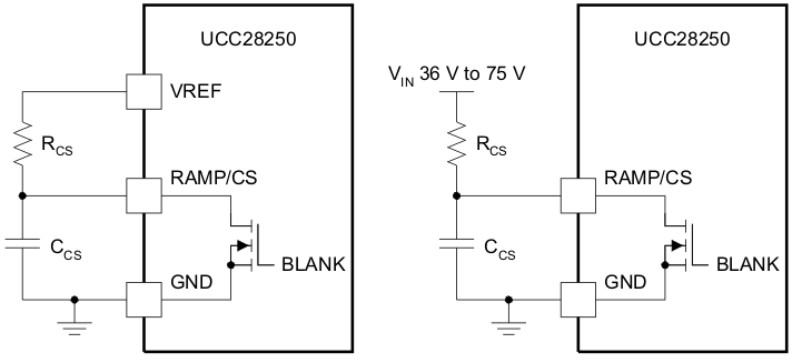 Figure 29. Fixed Ramp Generation/Ramp Generation With Input Voltage Feedforward
Voltage feed-forward can be achieved by driving RCS from line input VIN. The peak of RAMP/CS is proportional to VIN and output has have much faster line transient response. When the UCC28250 is used for the primary-side control, RAMP parameters are critical for the optimal prebiased start-up performance. Refer to the RAMP: Voltage Mode Control With Feed-Forward Operation for a detailed design procedure of choosing RCS.
If the line input cannot be easily accessed due to limited board area or other limitation, a RAMP signal with fixed peak voltage can be implemented by simply driving RCS from 3.3-V VREF (Figure 29).
7.3.7.2 CS: Current Mode Control
For current mode control, the RAMP/CS pin is driven by a signal representative of the transformer primary-side current. The current signal must have compatible input range of the COMP pin. As shown in Figure 30, the COMP pin voltage is used as the reference for peak current. The primary-side signals OUTA and OUTB are turned on by the internal clock signal and turned off when sensed peak current reaches the COMP pin voltage. Choose the current sense transformer turns ratio (1:n) and the burden resistor value (RB) based on the peak current at maximum load IMAX.

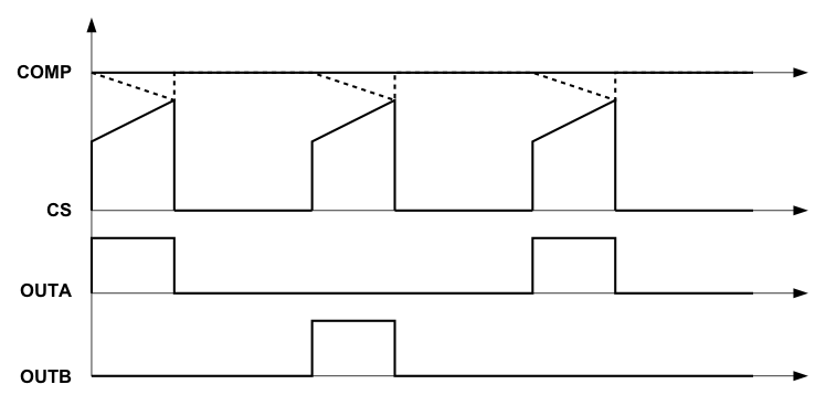 Figure 30. Peak Current Mode Control and PWM Generation
7.3.8 REF/EA+ (1/8)
REF/EA+ is the noninverting input of the UCC28250’s internal error amplifier.
When the UCC28250 is configured for secondary-side control, the internal error amplifier is used as the control loop error amplifier. Connect REF/EA+ directly to the VREF pin to provide the reference voltage for the feedback loop.
When the UCC28250 is configured for primary-side control, the error amplifier is connected as a voltage follower. Connect REF/EA+ to the opto-coupler output.
The voltage range on REF/EA+ pin is 0 V to 3.7 V.
7.3.9 FB/EA- (2/9)
FB/EA- is the inverting input of the UCC28250’s internal error amplifier.
When the UCC28250 is configured for secondary-side control, connect the output voltage sensing divider to this pin. The voltage divider can be selected according to the voltage on REF/EA+ pin. Referring to Figure 32, pick the lower resistor RO1 value arbitrarily, and choose the upper resistor RO2 value as:

Because the control loop gain is affected by voltage divider resistor values, choose an appropriate RO1 value so that the voltage loop DC gain is larger than 40 dB to prevent interference between the primary-side control loop and the SR control loop during start-up.
When the UCC28250 is sitting on the primary side, the error amplifier is connected as a voltage follower. Connect FB/EA- directly with COMP pin.
The maximum voltage allowed on FB/EA- pin is 3.7 V.
7.3.10 COMP (3/10)
The COMP pin is the internal error amplifier’s output and also the input signal for PWM comparator. The maximum input common voltage of the PWM comparator is 2.8 V. It is suggested to program the peak value of RAMP to be lower than 2.3 V. Otherwise, the voltage of COMP pin should be clamped to be lower than 2.8 V by external circuit to make the internal PWM comparator work properly. Figure 31 shows tan external circuit that is recommended for voltage clamp function. Both the primary-side switches’ duty cycle and secondary-side SRs’ duty cycle is controlled by the COMP pin voltage. At steady state, a higher COMP pin voltage results in a larger duty cycle for the primary-side switches and a smaller duty cycle on the SRs.
When the UCC28250 controller is set up for secondary-side control, connect the compensation network from the FB/EA- pin to the COMP pin.
For primary-side control, the error amplifier is connected as a voltage follower. Directly connect the COMP pin to the FB/EA- pin.
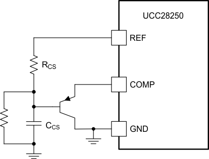 Figure 31. Comp Clamp Circuit
7.3.11 VSENSE (14/1)
The VSENSE pin is used to directly sense the output voltage and to feed it into a transconductance error amplifier. The measured voltage allows the UCC28250 to achieve optimal prebiased start-up performance.
When configured as a secondary-side controller, the output voltage is sensed and fed into the FB/EA- pin. The UCC28250 uses a conventional error amplifier approach to allow type III compensation. Therefore, the FB/EA- pin voltage always follows the REF/EA+ voltage. The FB/EA- pin does not reflect the true output voltage and therefore this dedicated VSENSE pin is required. The voltage divider connected to VSENSE is discussed in the Prebiased Start-Up Section.
When UCC28250 is set up as primary-side control, connect VSENSE pin to VREF.
7.3.12 SS (Soft Start Programming Pin) (13/20)
The soft-start circuit gradually increases the converter’s output voltage until steady state operation is reached. This reduces start-up stresses and current surge.
When the UCC28250 reaches its valid operating threshold, the SS pin capacitor is charged with a 27-µA current source. The UCC28250’s internal error amplifier noninverting terminal follows the SS pin voltage on REF/EA+ pin voltage depending on which one is lower. Hence, during soft start, the SS pin voltage is lower than REF/EA+. The internal error amplifier then uses the SS pin as its reference voltage, until the SS pin voltage rises above the REF/EA+ level. Once the SS pin voltage is above REF/EA+ voltage, soft-start time is considered finished.
The soft-start implementation scheme and timing is different, depending on the location of the UCC28250 with respect to the isolation barrier.
For secondary-side control, the internal error amplifier is used to achieve the voltage regulation. The REF/EA+ is connected to an external reference voltage, FB/EA- is connected to the voltage sensing divider, and the error amplifier’s output pin (COMP) is connected through a compensation filter back to the FB/EA- pin (Figure 32). In this case, the primary output’s start-up is a closed loop soft start (soft-start input reference of error amplifier). The output soft-start time is determined by the external capacitor connected at SS pin based on the internal 27-µA charging current and the voltage set at REF/EA+ pin.
Based on the soft-start time TSS, choose soft start capacitor CSS value as:

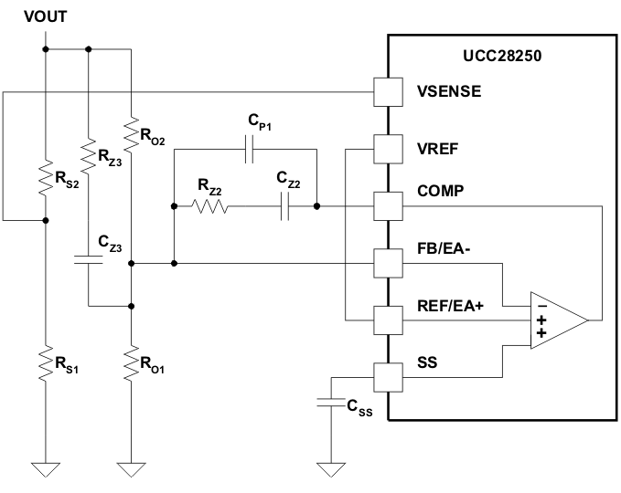 Figure 32. Error Amplifier EAMP Connections for Secondary-Side Control
For primary-side control, the internal error amplifier is connected as a buffer stage. In other words, the COMP pin is shorted to the FB/EA- pin, and the output of an external error amplifier is connected to the REF/EA+ pin through an optical coupler (Figure 33). In this case, the output start-up is an open loop soft start because the COMP follows the soft-start voltage instead of the voltage loop output. The soft-start time is still determined by external capacitor CSS and the 27-µA internal charge current. The voltage depends on the value of final COMP voltage which corresponds to the regulated primary output duty cycle. According to the desired soft start time and COMP pin voltage level at steady state, the SS pin capacitor can be calculated as:

After soft start, the voltage at SS pin is eventually clamped at around 4 V. Under fault conditions (UVLO, internal thermal shut down, OVP/OTP, hiccup mode), or when externally disabled, SS pin is pulled down to ground quickly by an internal switch with 2 kΩ on resistance to prepare for re-start. Pulling SS pin to ground externally shuts down the controller as well.
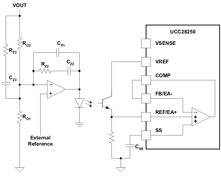 Figure 33. Error Amplifier EAMP Connections for Primary-Side Control
7.3.13 ILIM (Current Limit for Cycle-By-Cycle Overcurrent Protection) (17/4)
Cycle-by-cycle current limit is accomplished using the ILIM pin for current mode control or for voltage mode control. The input to the ILIM pin represents the primary current information. If the voltage sensed at ILIM pin exceeds 0.5 V, the current sense comparator terminates the pulse of output OUTA or OUTB. If the high current condition persists, the controller operates in a cycle-by-cycle current limit mode with duty cycle determined by the current sense comparator instead of the PWM comparator. ILIM pin is pulled down by an internal switch at the rising edge of every clock cycle. This internal switch remains on for an additional 70 ns after OUTA or OUTB goes high to blank leading edge transient noise in the current sensing loop. This reduces the filtering requirements at the ILIM pin and improves the current sense response time.
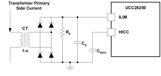 Figure 34. Current Limit Circuit
Once the over current protection level IPK is selected, the current transformer turns ratio and the burden resistor value can be decided as:

In this equation, current transformer turns ratio is 1:n and RS is the burden resistor value.
Some filtering capacitance is required to reduce the sensing noise. Choose the RC constant at about 100 ns, and calculate the capacitor value as:

The cycle-by-cycle current limit operation time before all four outputs shut down can be programmed by external capacitor CHICC at HICC pin. (See HICC pin description)
7.3.14 HICC (10/17)
The cycle-by-cycle current limit operation time before all four outputs shut down can be programmed by an external capacitor CHICC from HICC pin to ground, as shown in Figure 34. Once all four outputs are shutdown, controller goes into hiccup cycle which is about 100 times of the cycle-by-cycle current limit shut-down delay time. A 1-mA internal current source charges HICC pin up to 2.4 V, then the HICC pin is discharged by a 2.7-µA internal current source to generate long hiccup restart time until HICC reaches 0.3 V. Based on the system requirement, once the cycle-by-cycle current limit delay time TOC(delay) is selected, the HICC pin capacitor CHICC can be selected based on the equation

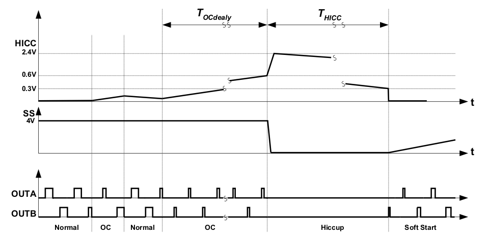 Figure 35. Cycle-by-Cycle Current Limit Delay Timer and Hiccup Restart Timer
As shown in Figure 35, cycle-by-cycle current limiting shut-down delay time is:

And hiccup-restart-time THICC is equal to:

As soon as the outputs are shut-down, the SS pin is pulled to ground internally until the hiccup restart timer is reset after time duration THICC.
7.3.15 OVP/OTP (19/6)
The OVP/OTP pin provides multiple fault protection functions. If the voltage on the OVP/OTP pin exceeds 0.7 V, a fault shutdown occurs. All outputs stop switching and stay off (low) during the shutdown, and the SS pin is pulled to ground internally. Once the fault condition is cleared (that is, OVP/OTP voltage drops below 0.7 V), the UCC28250 enters hiccup mode. A soft-start cycle begins after the hiccup cycle is finished. An internal 11-µA switched current source is used to create hysteresis.
If the external resistor divider runs from line voltage VIN, a line overvoltage protection is implemented.
If the external resistor divider runs from the output voltage, output overvoltage fault protection is achieved. Figure 36 shows the overvoltage protection external configuration at the OVP/OTP pin.
According to the protection threshold VR and recovery threshold VF, choose an arbitrary R2 value. To ensure a realistic solution, R2 must meet the following:

The other two resistors, R1 and R3 can be calculated.


If the external resistor divider runs from 3.3-V VREF, and replaces R2 with a positive temperature coefficient (PTC) thermistor, an overtemperature fault protection with programmable hysteresis is accomplished (Figure 37). Choose an arbitrary PTC value, which has a resistance as RPTC1 at protection temperature and resistance as RPTC2 at recovery temperature. Because of its positive temperature coefficient, RPTC1 is larger than RPTC2. To ensure an available solution, RPTC1 and RPTC2 need to meet the criteria.

And resistors R1 and R3 can be calculated as:


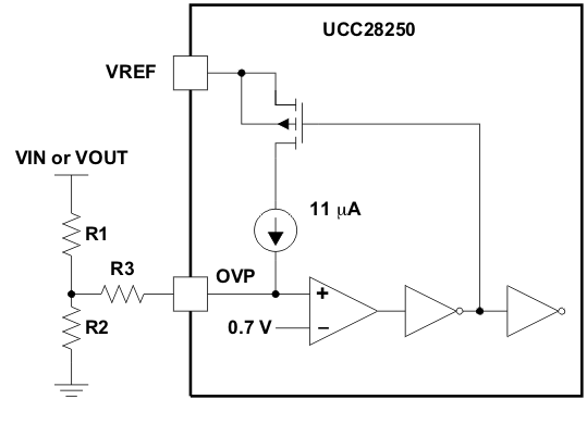 Figure 36. Overvoltage Protection
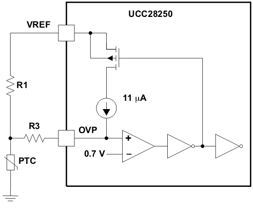 Figure 37. Overtemperature Protection
Figure 38 shows an external configuration using the OVP/OTP pin to achieve both overvoltage and overtemperature protection. Follow the same design procedure for the OVP setting to choose R1, R2, and R3. Choose an NTC value at protection temperature much smaller than R1 and with the resistance at protection temperature as RNTC1, and recover temperature as RNTC2. The R4 value can be calculated as:

Because of the interaction between the two voltage dividers, overtemperature protection thresholds move slightly with the different input voltages.
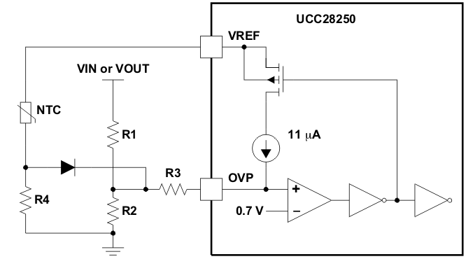 Figure 38. Overvoltage and Overtemperature Protection With Single OVP Pin
7.3.16 OUTA (9/16) and OUTB (8/15)
OUTA and OUTB are the primary-side switch control signals. With the 0.2-A peak current capability, an external gate driver is required.
7.3.17 SRA (7/14) and SRB (6/13)
SRA and SRB are the synchronous rectifier control signals. With the 0.2-A peak current capability, an external gate driver is required.
7.3.18 GND (4/11)
GND pin is the ground reference for the whole device. Tie all the signal returns to this pin.
7.4 Device Functional Modes
The UCC28250 can be controlled using either voltage mode or current mode. RAMP/CS is a multi-function pin used either to generate the ramp signal for voltage mode control or to sense current for current mode control. Refer to RAMP/CS (PWM Ramp Input or Current Sense Input) (16/3) for the details.
