SLUS646K November 2005 – August 2015 UCC28600
PRODUCTION DATA.
- 1 Features
- 2 Applications
- 3 Description
- 4 Revision History
- 5 Pin Configuration and Functions
- 6 Specifications
- 7 Detailed Description
- 8 Application and Implementation
- 9 Power Supply Recommendations
- 10Layout
- 11Device and Documentation Support
- 12Mechanical, Packaging, and Orderable Information
6 Specifications
6.1 Absolute Maximum Ratings
over operating free-air temperature range (unless otherwise noted) (1)| MIN | MAX | UNIT | ||
|---|---|---|---|---|
| VDD | Supply voltage range, IDD < 20 mA | 32 | V | |
| IDD | Supply current | 20 | mA | |
| IOUT(sink) | Output sink current (peak) | 1.2 | A | |
| IOUT(source) | Output source current (peak) | –0.8 | A | |
| Analog inputs: FB, CS, SS | –0.3 | 6.0 | V | |
| VOVP | –1.0 | 6.0 | V | |
| IOVP(source) | –1.0 | mA | ||
| VSTATUS | VDD = 0 V to 30 V | 30 | V | |
| Power dissipation, SOIC-8 package, TA = 25°C | 650 | mW | ||
| TLEAD | Lead temperature 1,6 mm (1/16 inch) from case for 10 seconds | 300 | °C | |
| TJ | Operating junction temperature | –55 | 150 | °C |
| Tstg | Storage temperature | –65 | 150 | °C |
(1) Stresses beyond those listed under Absolute Maximum Ratings may cause permanent damage to the device. These are stress ratings only, which do not imply functional operation of the device at these or any other conditions beyond those indicated under Recommended Operating Conditions. Exposure to absolute-maximum-rated conditions for extended periods may affect device reliability.
6.2 ESD Ratings
| VALUE | UNIT | ||||
|---|---|---|---|---|---|
| V(ESD) | Electrostatic discharge | Human body model (HBM), per ANSI/ESDA/JEDEC JS-001, all pins (1) | ±2000 | V | |
| Charged device model (CDM), per JEDEC specification JESD22-C101, all pins (2) | ±1500 | V | |||
(1) JEDEC document JEP155 states that 500-V HBM allows safe manufacturing with a standard ESD control process.
(2) JEDEC document JEP157 states that 250-V CDM allows safe manufacturing with a standard ESD control process.
6.3 Recommended Operating Conditions
over operating free-air temperature range (unless otherwise noted)| MIN | NOM | MAX | UNIT | ||
|---|---|---|---|---|---|
| VDD | Input voltage | 21 | V | ||
| CVDD | VDD bypass capacitor | 0.1 | 1.0 | μF | |
| CFB | FB filter capacitor | 390 | pF | ||
| TJ | Operating junction temperature | –40 | 105 | °C | |
6.4 Thermal Information
| THERMAL METRIC (1) | UCC28600 | UNIT | |
|---|---|---|---|
| D (SOIC) | |||
| 8 PINS | |||
| RθJA | Junction-to-ambient thermal resistance | 108.9 | °C/W |
| RθJC(top) | Junction-to-case (top) thermal resistance | 55.5 | °C/W |
| RθJB | Junction-to-board thermal resistance | 48.9 | °C/W |
| ψJT | Junction-to-top characterization parameter | 10.5 | °C/W |
| ψJB | Junction-to-board characterization parameter | 48.5 | °C/W |
(1) For more information about traditional and new thermal metrics, see the Semiconductor and IC Package Thermal Metrics application report, SPRA953.
6.5 Electrical Characteristics
VDD = 15 V, 0.1-μF capacitor from VDD to GND, 3.3-nF capacitor from SS to GND charged over 3.5 V, 500-Ω resistor from OVP to –0.1 V, FB = 4.8 V, STATUS = not connected, 1-nF capacitor from OUT to GND, CS = GND, TA = –40°C to +105°C, (unless otherwise noted)| PARAMETER | TEST CONDITIONS | MIN | TYP | MAX | UNIT | |
|---|---|---|---|---|---|---|
| ISTARTUP | Start-up current | VDD = VUVLO –0.3 V | 12 | 25 | μA | |
| ISTANDBY | Standby current | VFB = 0 V | 350 | 550 | μA | |
| IDD | Operating current | Not switching | 2.5 | 3.5 | mA | |
| 130 kHz, QR mode | 5.0 | 7.0 | mA | |||
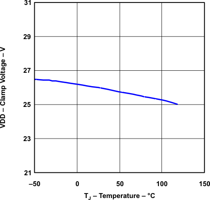
| VDD clamp | FB = GND, IDD = 10 mA | 21 | 26 | 32 | V | |
| UNDERVOLTAGE LOCKOUT | ||||||
| VDD(uvlo) | Start-up threshold | VDD increasing | 10.3 | 13.0 | 15.3 | V |
| VDD(uvlo) | Stop threshold | VDD decreasing | 6.3 | 8 | 9.3 | V |
| ΔVDD(uvlo) | Hysteresis | 4.0 | 5.0 | 6.0 | V | |
| PWM (RAMP) (2) | ||||||
| DMIN | Minimum duty cycle | VSS = GND, VFB = 2 V | 0% | |||
| DMAX | Maximum duty cycle | QR mode, fS = max, (open loop) | 99% | |||
| OSCILLATOR (OSC) | ||||||
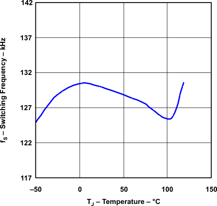
| fQR(max) | Maximum QR and DCM frequency | 117 | 130 | 143 | kHz | |
| fQR(min) | Minimum QR and FFM frequency | VFB = 1.3 V | 32 | 40 | 48 | kHz |
| fSS | Soft start frequency | VSS = 2.0 V | 32 | 40 | 48 | kHz |
| dTS/dFB | VCO gain | TS for 1.6 V < VFB < 1.8 V | –38 | –30 | –22 | μs/V |
| FEEDBACK (FB) | ||||||
| RFB | Feedback pullup resistor | 12 | 20 | 28 | kΩ | |
| VFB | FB, no load | QR mode | 3.30 | 4.87 | 6.00 | V |
| Green-mode ON threshold | VFB threshold | 0.3 | 0.5 | 0.7 | V | |
| Green-mode OFF threshold | VFB threshold | 1.2 | 1.4 | 1.6 | V | |
| Green-mode hysteresis | VFB threshold | 0.7 | 0.9 | 1.1 | V | |
| FB threshold burst-ON | VFB during green mode | 0.3 | 0.5 | 0.7 | V | |
| FB threshold burst-OFF | VFB during green mode | 0.5 | 0.7 | 0.9 | V | |
| Burst Hysteresis | VFB during green mode | 0.13 | 0.25 | 0.42 | V | |
| STATUS | ||||||
| RDS(on) | STATUS on resistance | VSTATUS = 1 V | 1.0 | 2.4 | 3.8 | kΩ |
| ISTATUS(leakage) | STATUS leakage/off current | VFB = 0.44 V, VSTATUS = 15 V | –0.1 | 2.0 | μA | |
| CURRENT SENSE (CS) (2) | ||||||
| ACS(FB) | Gain = ΔVFB / ΔVCS | QR mode | 2.5 | V/V | ||
| Shutdown threshold | VFB = 2.4 V, VSS = 0 V | 1.13 | 1.25 | 1.38 | V | |
| CS discharge impedance | CS = 0.1 V, VSS = 0 V | 25 | 115 | 250 | Ω | |
| VCS(os) | CS offset | SS mode, VSS ≤ 2.0 V | 0.35 | 0.40 | 0.45 | V |
| POWER LIMIT (PL) (2) | ||||||
| IPL(cs) | CS current | OVP = –300 μA | –165 | –150 | –135 | μA |
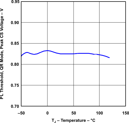
| Peak CS voltage | QR mode | 0.70 | 0.81 | 0.92 | V | |
| VPL | PL threshold | Peak CS voltage + CS offset | 1.05 | 1.20 | 1.37 | V |
| SOFT START (SS) | ||||||
| ISS(chg) | Softstart charge current | VSS = GND | –8.3 | –6.0 | –4.5 | μA |
| ISS(dis) | Softstart discharge current | VSS = 0.5 V | 2.0 | 5.0 | 10 | mA |
| VSS | Switching ON threshold | Output switching start | 0.8 | 1.0 | 1.2 | V |
| OVERVOLTAGE PROTECTION (OVP) | ||||||
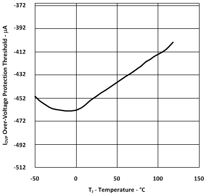
| IOVP(line) | Line overvoltage protection | IOVP threshold, OUT = HI | –512 | –450 | –370 | μA |
| VOVP(on) | OVP voltage at OUT = HIGH | VFB = 4.8 V, VSS = 5.0 V, IOVP(on), = –300 μA |
–125 | –25 | mV | |
| VOVP(load) | Load overvoltage protection | VOVP threshold, OUT = LO | 3.37 | 3.75 | 4.13 | V |
| THERMAL PROTECTION (TSP) | ||||||
| Thermal shutdown (TSP) temperature (1) | 130 | 140 | 150 | °C | ||
| Thermal shutdown hysteresis | 15 | °C | ||||
(1) Ensured by design. Not production tested.
(2) RCST and CCST are not connected in the circuit for maximum and minimum duty cycle tests, current sense tests, and power limit tests.
Timing Requirements
| MIN | NOM | MAX | UNIT | ||
|---|---|---|---|---|---|
| CURRENT SENSE (CS) (2) | |||||
| CS to output delay time (power limit), CS = 1.0 VPULSE | 100 | 175 | 300 | ns | |
| CS to output delay time (over current fault), CS = 1.45 VPULSE | 50 | 100 | 150 | ns | |
| OUT | |||||
| tRISE | Rise time, 10% to 90% of 13-V typical OUT clamp | 50 | 75 | ns | |
| tFALL | Fall time | 10 | 20 | ns | |
6.6 Typical Characteristics


