ZHCS310G JANUARY   2009  – September 2015 UCC28610

PRODUCTION DATA.  

  1. 特性
  2. 应用
  3. 说明
  4. 修订历史记录
  5. Pin Configuration and Functions
  6. Specifications
    1. 6.1 Absolute Maximum Ratings
    2. 6.2 ESD Ratings
    3. 6.3 Recommended Operating Conditions
    4. 6.4 Thermal Information
    5. 6.5 Electrical Characteristics
    6. 6.6 Typical Characteristics
  7. Detailed Description
    1. 7.1 Overview
    2. 7.2 Functional Block Diagram
    3. 7.3 Feature Description
      1. 7.3.1 Fault Recovery
      2. 7.3.2 Maximum On-Time and Brown Out
      3. 7.3.3 External Shutdown Using the MOT Pin
      4. 7.3.4 Overvoltage Detection
      5. 7.3.5 Solving for High Frequency Ringing
        1. 7.3.5.1 Identification of High Frequency Ringing
        2. 7.3.5.2 Avoid HF Ringing
        3. 7.3.5.3 Ferrite Chip or Bead Solution
        4. 7.3.5.4 DRV Capacitor Solution
        5. 7.3.5.5 Gate Turn-Off Resistor Solution
      6. 7.3.6 Thermal Shutdown
    4. 7.4 Device Functional Modes
  8. Application and Implementation
    1. 8.1 Application Information
      1. 8.1.1 Transformer Selection
      2. 8.1.2 Cascode Bias and Start-Up
      3. 8.1.3 Feedback Function
      4. 8.1.4 Modulation Modes
      5. 8.1.5 Primary Current Sense
      6. 8.1.6 Zero Crossing Detection
      7. 8.1.7 Green Mode Operation
      8. 8.1.8 Maximum Converter Power Limitation
      9. 8.1.9 Minimum Converter Power Limitation
    2. 8.2 Typical Application
      1. 8.2.1 Design Requirements
      2. 8.2.2 Detailed Design Procedure
        1. 8.2.2.1 Input Bulk Capacitance and Minimum Bulk Voltage
        2. 8.2.2.2 Transformer Selection
        3. 8.2.2.3 Feedback Function
      3. 8.2.3 Application Curves
  9. Power Supply Recommendations
  10. 10Layout
    1. 10.1 Layout Guidelines
    2. 10.2 Layout Example
  11. 11器件和文档支持
    1. 11.1 社区资源
    2. 11.2 商标
    3. 11.3 静电放电警告
    4. 11.4 Glossary
  12. 12机械、封装和可订购信息

封装选项

机械数据 (封装 | 引脚)
散热焊盘机械数据 (封装 | 引脚)
订购信息

Layout

Layout Guidelines

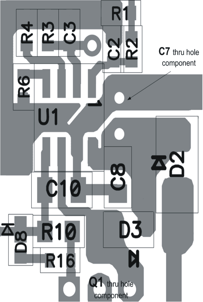
It is possible to design a power supply on a single layer board using the UCC28610. Figure 43 and Figure 44 show an example of a typical layout and design, respectively. Proper use of ground planes can solve EMI and thermal problems. For best results, create a quiet ground plane for the components associated with pins 1 through 4. This offers shielding for the control signals. Also, do not extend the ground plane under heat sinks, thermistors or snubbers so that these components do not heat the UCC28610.

Layout Example

UCC28610 fig33_lus888.gif Figure 43. Typical Layout of the Device on a Single Layer PCB

NOTE

The reference designators correspond to the components shown in the schematic of Figure 44.
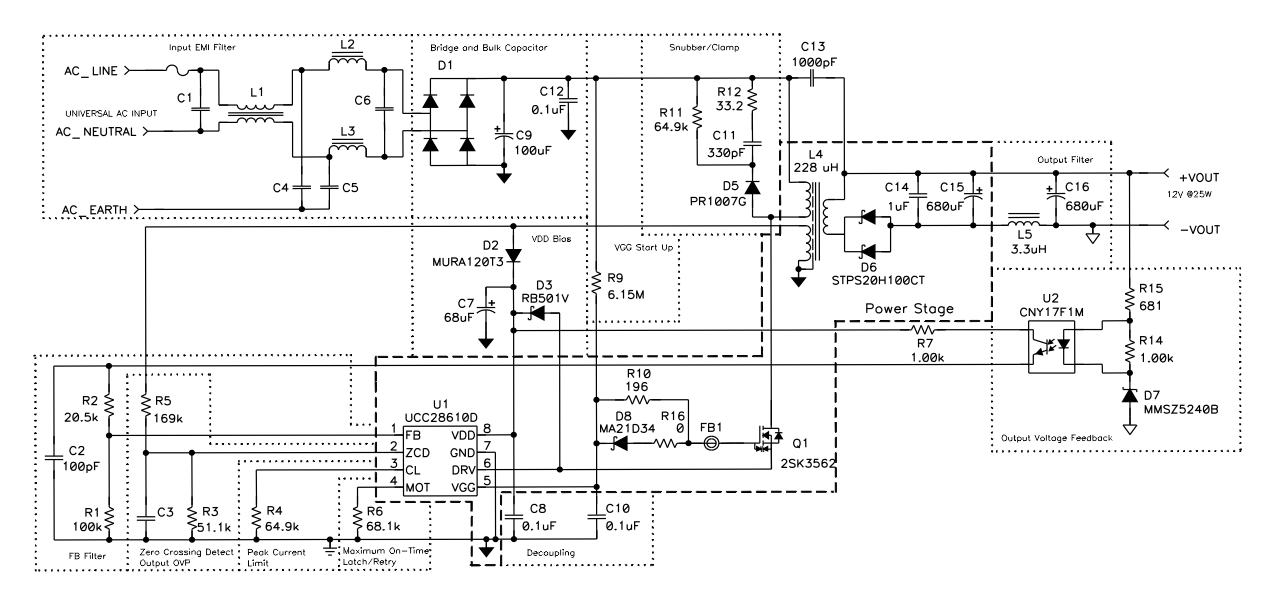
UCC28610 fig34_lus888.gif Figure 44. Typical Design Schematic