ZHCSC62D March 2014 – December 2017 UCC28630 , UCC28631 , UCC28632 , UCC28633 , UCC28634
PRODUCTION DATA.
- 1 特性
- 2 应用
- 3 说明
- 4 修订历史记录
- 5 Device Comparison Table
- 6 Pin Configuration and Functions
- 7 Specifications
-
8 Detailed Description
- 8.1 Overview
- 8.2 Functional Block Diagram
- 8.3
Feature Description
- 8.3.1 High-Voltage Current Source Start-Up Operation
- 8.3.2 AC Input UVLO / Brownout Protection
- 8.3.3 Active X-Capacitor Discharge (UCC28630 and UCC28633 only)
- 8.3.4 Magnetic Input and Output Voltage Sensing
- 8.3.5 Fixed-Point Magnetic Sense Sampling Error Sources
- 8.3.6 Magnetic Sense Resistor Network Calculations
- 8.3.7 Magnetic Sensing: Power Stage Design Constraints
- 8.3.8 Magnetic Sense Voltage Control Loop
- 8.3.9 Peak Current Mode Control
- 8.3.10 IPEAK Adjust vs. Line
- 8.3.11 Primary-Side Constant-Current Limit (CC Mode)
- 8.3.12 Primary-Side Overload Timer (UCC28630 only)
- 8.3.13 Overload Timer Adjustment (UCC28630 only)
- 8.3.14 CC-Mode IOUT(lim) Adjustment
- 8.3.15 Fault Protections
- 8.3.16 Pin-Fault Detection and Protection
- 8.3.17 Over-Temperature Protection
- 8.3.18 External Fault Input
- 8.3.19 External SD Pin Wake Input (except UCC28633)
- 8.3.20 External Wake Input at VSENSE Pin (UCC28633 Only)
- 8.3.21 Mode Control and Switching Frequency Modulation
- 8.3.22 Frequency Dither For EMI (except UCC28632)
- 8.4 Device Functional Modes
-
9 Applications and Implementation
- 9.1 Application Information
- 9.2
Typical Application
- 9.2.1 Notebook Adapter, 19.5 V, 65 W
- 9.2.2 UCC28630 Application Schematic
- 9.2.3 Design Requirements
- 9.2.4
Detailed Design Procedure
- 9.2.4.1 Custom Design With WEBENCH® Tools
- 9.2.4.2 Input Bulk Capacitance and Minimum Bulk Voltage
- 9.2.4.3 Transformer Turn Ratio
- 9.2.4.4 Transformer Magnetizing Inductance
- 9.2.4.5 Current Sense Resistor RCS
- 9.2.4.6 Transformer Constraint Verification
- 9.2.4.7 Transformer Selection and Design
- 9.2.4.8 Slope Compensation Verification
- 9.2.4.9 Power MOSFET and Output Rectifier Selection
- 9.2.4.10 Output Capacitor Selection
- 9.2.4.11 Calculation of CC Mode Limit Point
- 9.2.4.12 VDD Capacitor Selection
- 9.2.4.13 Magnetic Sense Resistor Network Selection
- 9.2.4.14 Output LED Pre-Load Resistor Calculation
- 9.2.5 External Wake Pulse Calculation at VSENSE Pin (UCC28633 Only)
- 9.2.6 Energy Star Average Efficiency and Standby Power
- 9.2.7 Application Performance Plots
- 9.3 Dos and Don'ts
- 10Power Supply Recommendations
- 11Layout
- 12器件和文档支持
- 13机械、封装和可订购信息
8.3.3.1 Improved Performance with UCC28630 and UCC28633
In order to reduce standby power and eliminate the standing loss associated with the conventional discharge resistors, the UCC28630 and the UCC28633 devices incorporate active X-capacitor discharge circuitry. This circuit periodically monitors the voltage across the X-capacitor to detect any possible DC-condition (which would indicate that AC mains disconnection has occurred), and then discharges the voltage across the X-capacitor using the internal HV current source. The X-capacitor discharge function discharges the X-capacitor to the SELV 60-V level in 1 s (as long as the design considerations discussed in this section are followed).
The device internally monitors the current into the HV pin to determine if the voltage across the X-capacitor in the EMI filter has a sufficient AC ripple component. If insufficient AC content is detected, then a DC condition is internally flagged. This causes the controller to enter low-power mode for the reset period (tRESET(short)), followed by bias voltage discharge to the reset level (VDD(reset)) , and then the start-up HV current source turns on again to effectively discharge the X-capacitor by transferring charge to the VDD reservoir capacitor.
Because the device monitors the HV pin to detect a DC condition on the X-capacitor, the system cannot operate with DC input to the HV pin. Instead, the HV pin must be connected to an AC source only. The device interprets any DC input on the HV pin as DC across the X-capacitor, indicating an AC-disconnect event. This causes a repeating cycle of start-up and shutdown. The device requires an external 200-kΩ of resistance on the HV pin, to limit the current to a level below the saturation point of the internal HV current source. This limit produces a HV input current that is approximately proportional to AC line, so that the AC content can be sensed.
The size of the X-capacitor that can be discharged depends on the VDD energy storage capacitor. Assuming the worst case, a maximum X-capacitor disconnect voltage could be at the peak of 264 VRMS, and assuming that it should be discharged down to 60-V SELV level, the minimum allowed VDD capacitor can be sized based on the worst case VDD(reset) and VDD(start) levels as described in Equation 3.

For example, for a 330-nF X-capacitor value, the required VDD capacitor is 15.9 µF, so a 22-µF capacitor suffices.

In order to reduce the power consumption from the high voltage AC line, the device pulses current into the HV pin at a low frequency with very low duty-cycle. The HV current source on-time (tON(HV)) , repeats at intervals of tSMP(HV). Moreover, the pulsing occurs in bursts, with a time delay between bursts. The sampling occurs in bursts of 21, at intervals of tSMP(HV), with a wait time of tWAIT(HV) between bursts. This reduces the effective average duty-cycle to a very low value (approximately 0.2%), and minimizes the overhead of X-capacitor sampling current and device bias consumption overhead to approximately 2 mW of extra standby consumption at high-line 230 VAC.
The device enables the X-capacitor monitor in latched fault mode, and in light-load regions where the power level is below PLL(%), as a percentage of the nominal rated level. Above the PLL(%) level, the X-capacitor monitor is disabled. At this load level the bulk capacitor discharges at a rate that is sufficient to also discharge the X-capacitor, which appears in parallel with the bulk capacitor once the bulk voltage drops far enough to forward bias the bridge rectifier diodes. In this case ensure that the bulk capacitance value is not too large for the power level desired, which in-turn ensures that the bulk capacitor discharge rate is fast enough to discharge the X-capacitor to meet the 1-s discharge target. This can be calculated in Equation 5.

Assuming a worst case AC disconnect at the peak at 264 VRMS (373 VPK), and a requirement to discharge to SELV level of 60 V in tXCAP(dis) of 1 s, for a PNOM of 65 W at 87% efficiency, this is calculated in Equation 6.

Once the bulk capacitance value is chosen, also ensure that when the bulk capacitor has been discharged down to the line UV ACOFF threshold, that it continues to discharge to an acceptable level during the line UV persistence delay time (tUV(delay)) as shown in Equation 7.
Again, taking the example above:

Once the first constraint is satisfied, the second one is also automatically met.
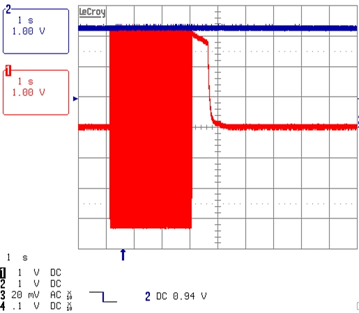
 Figure 19. X-Capacitor Discharge Activation, at 230 VAC, No Load
 (red = X-capacitor, blue = bulk-capacitor, both 100 V/div)
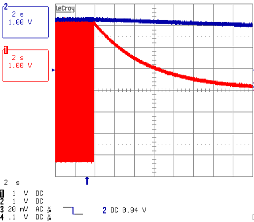
 Figure 20. X-Capacitor Decay Rate Without Active Discharge
 (time constant dominated by 20-MΩ probe impedance)
(red = X-capacitor, blue = bulk-capacitor, both 100 V/div)
