ZHCSC62D March 2014 – December 2017 UCC28630 , UCC28631 , UCC28632 , UCC28633 , UCC28634
PRODUCTION DATA.
- 1 特性
- 2 应用
- 3 说明
- 4 修订历史记录
- 5 Device Comparison Table
- 6 Pin Configuration and Functions
- 7 Specifications
-
8 Detailed Description
- 8.1 Overview
- 8.2 Functional Block Diagram
- 8.3
Feature Description
- 8.3.1 High-Voltage Current Source Start-Up Operation
- 8.3.2 AC Input UVLO / Brownout Protection
- 8.3.3 Active X-Capacitor Discharge (UCC28630 and UCC28633 only)
- 8.3.4 Magnetic Input and Output Voltage Sensing
- 8.3.5 Fixed-Point Magnetic Sense Sampling Error Sources
- 8.3.6 Magnetic Sense Resistor Network Calculations
- 8.3.7 Magnetic Sensing: Power Stage Design Constraints
- 8.3.8 Magnetic Sense Voltage Control Loop
- 8.3.9 Peak Current Mode Control
- 8.3.10 IPEAK Adjust vs. Line
- 8.3.11 Primary-Side Constant-Current Limit (CC Mode)
- 8.3.12 Primary-Side Overload Timer (UCC28630 only)
- 8.3.13 Overload Timer Adjustment (UCC28630 only)
- 8.3.14 CC-Mode IOUT(lim) Adjustment
- 8.3.15 Fault Protections
- 8.3.16 Pin-Fault Detection and Protection
- 8.3.17 Over-Temperature Protection
- 8.3.18 External Fault Input
- 8.3.19 External SD Pin Wake Input (except UCC28633)
- 8.3.20 External Wake Input at VSENSE Pin (UCC28633 Only)
- 8.3.21 Mode Control and Switching Frequency Modulation
- 8.3.22 Frequency Dither For EMI (except UCC28632)
- 8.4 Device Functional Modes
-
9 Applications and Implementation
- 9.1 Application Information
- 9.2
Typical Application
- 9.2.1 Notebook Adapter, 19.5 V, 65 W
- 9.2.2 UCC28630 Application Schematic
- 9.2.3 Design Requirements
- 9.2.4
Detailed Design Procedure
- 9.2.4.1 Custom Design With WEBENCH® Tools
- 9.2.4.2 Input Bulk Capacitance and Minimum Bulk Voltage
- 9.2.4.3 Transformer Turn Ratio
- 9.2.4.4 Transformer Magnetizing Inductance
- 9.2.4.5 Current Sense Resistor RCS
- 9.2.4.6 Transformer Constraint Verification
- 9.2.4.7 Transformer Selection and Design
- 9.2.4.8 Slope Compensation Verification
- 9.2.4.9 Power MOSFET and Output Rectifier Selection
- 9.2.4.10 Output Capacitor Selection
- 9.2.4.11 Calculation of CC Mode Limit Point
- 9.2.4.12 VDD Capacitor Selection
- 9.2.4.13 Magnetic Sense Resistor Network Selection
- 9.2.4.14 Output LED Pre-Load Resistor Calculation
- 9.2.5 External Wake Pulse Calculation at VSENSE Pin (UCC28633 Only)
- 9.2.6 Energy Star Average Efficiency and Standby Power
- 9.2.7 Application Performance Plots
- 9.3 Dos and Don'ts
- 10Power Supply Recommendations
- 11Layout
- 12器件和文档支持
- 13机械、封装和可订购信息
9.2.5 External Wake Pulse Calculation at VSENSE Pin (UCC28633 Only)
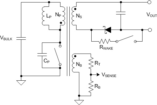
The typical application circuit of Figure 39 may be redrawn as a simplified equivalent circuit as shown in Figure 45. In this equivalent circuit, the capacitor CP is the total parasitic capacitance (MOSFET Coss, transformer capacitance, etc), and resistance RWAKE is the effective internal resistance of the UCC24650 WAKE pin to GND pin when the internal WAKE pull-down is active (see UCC24650 detailed datasheet specifications).
If all the elements on the primary and secondary of the transformer are referred to the bias winding, this can be further simplified as in Figure 46.
 Figure 45. Simplified Equivalent Circuit of Wake Event with UCC24650
  Figure 46. Bias-Referred Simplified Equivalent Circuit of Wake Event with UCC24650
 Thus, knowing LP and CP, the power stage impedance ZLC(bias) (reflected to the bias winding) may be calculated from Equation 66, and the effective wake resistance can be referred to the bias winding using Equation 67. The wake pulse amplitude can be calculated from Equation 68. If CP is not known, it can be measured by observing the resonant ring period at the primary drain node, TRES, and calculating CP from Equation 69. Worst case values should be used to estimate the worst case minimum wake pulse amplitude at the VSENSE pin. It should also be noted that any filter cap on the VSENSE pin (including internal parasitic pin capacitance) adds an RC filter in conjunction with the Thevenin resistance of the VSENSE divider, RT, RB; this delays and further attenuate the wake pulse amplitude. Additionally, the internal wake comparator requires some over-drive to trip, and exhibits propagation delay that depends on the amount of overdrive. So some margin should be allowed in the wake pulse amplitude to ensure that the minimum wake pulse can adequately overdrive the internal wake comparator. A margin of at least 20% over the threshold VSENSE(wake) is recommended.


If the worst case wake pulse amplitude is too low, then the UCC24650 WAKE output can be augmented with an external PNP circuit Q1, R1 and R2, as shown in Figure 40. This circuit reduces the effective wake resistance to ground, so that a larger proportion of the output voltage appears across the transformer secondary pins when the UCC24650 WAKE activates.
Using the UCC28630EVM-572, (TI Literature Number SLUUAX9) circuit parameters from Figure 44, the nominal wake pulse amplitude at the VSENSE pin can be estimated. Of course, the rectifying diode D7 in Figure 44 would need to be relocated to return end of the secondary winding (pins 10, 11) to allow UCC24650 to be deployed.
From observation of the DCM ringing period, the period TRES was found to be 1.138 μs. From Equation 69, CP is estimated:

From Equation 66, the power circuit impedance is:

The WAKE pin resistance RWAKE can be determined form the UCC24650 datasheet; for now a nominal value of 400 Ω is assumed. Referred to the bias winding (scaled by (NB/NS)2), this becomes 178 Ω. Similarly ΔWAKE% can be determined from the UCC24650 datasheet; for now, a value of 97% is assumed. From Equation 68, the wake pulse amplitude can be calculated:
In this case, the VSENSE wake pulse amplitude would be insufficient to trip the internal wake comparator. If the power stage had higher LP, or lower CP, a larger wake pulse would be produced.
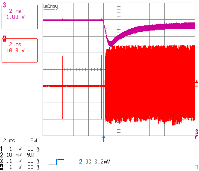
Alternatively, the effective wake resistance RWAKE may be reduced by adding the PNP circuit per Figure 40. This has been verified using Q1 = FMMTA92 PNP transistor, R1= 100 Ω and R2 = 2.2 kΩ. A wake pulse amplitude of almost 2 VPK was produced at the VSENSE pin, giving generous margin to the internal threshold VSENSE(wake). The observed waveforms are shown in Figure 47 for a worst case 0% to 100% (65 W) load transient (where the PWM is at FMIN). The PWM is re-activated when VOUT has dropped by ~3%, rather waiting for the next timed wake-up (~5 ms later).
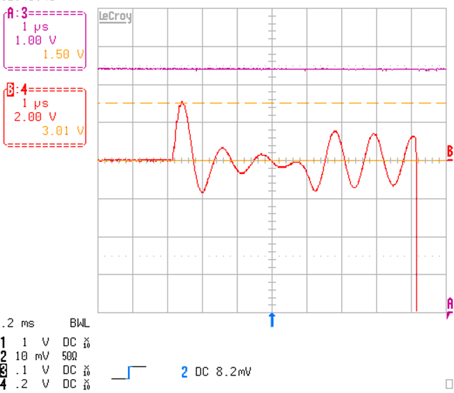
Figure 48 shows a zoomed waveform of the wake pulsing ringing as measured on the bias winding. It can be seen that the peak level is approximately 3 VPK, which would produce a pulse of approximately 1.8 V at the VSENSE pin (scaled by VSENSE divider resistors RT and RB). As noted in Test and Debug Recommendations, the VSENSE pin should never be directly probed, doing so affects the regulation setpoint.
 Figure 47. Observed Output Voltage (Ch3) and Bias Winding (Ch4)
 (showing wake event generated by UCC24650)
 Figure 48. Zoom In of Wake-Pulse Ringing
 (observed across bias winding (ChB) generated by UCC24650)
