ZHCSC62D March 2014 – December 2017 UCC28630 , UCC28631 , UCC28632 , UCC28633 , UCC28634
PRODUCTION DATA.
- 1 特性
- 2 应用
- 3 说明
- 4 修订历史记录
- 5 Device Comparison Table
- 6 Pin Configuration and Functions
- 7 Specifications
-
8 Detailed Description
- 8.1 Overview
- 8.2 Functional Block Diagram
- 8.3
Feature Description
- 8.3.1 High-Voltage Current Source Start-Up Operation
- 8.3.2 AC Input UVLO / Brownout Protection
- 8.3.3 Active X-Capacitor Discharge (UCC28630 and UCC28633 only)
- 8.3.4 Magnetic Input and Output Voltage Sensing
- 8.3.5 Fixed-Point Magnetic Sense Sampling Error Sources
- 8.3.6 Magnetic Sense Resistor Network Calculations
- 8.3.7 Magnetic Sensing: Power Stage Design Constraints
- 8.3.8 Magnetic Sense Voltage Control Loop
- 8.3.9 Peak Current Mode Control
- 8.3.10 IPEAK Adjust vs. Line
- 8.3.11 Primary-Side Constant-Current Limit (CC Mode)
- 8.3.12 Primary-Side Overload Timer (UCC28630 only)
- 8.3.13 Overload Timer Adjustment (UCC28630 only)
- 8.3.14 CC-Mode IOUT(lim) Adjustment
- 8.3.15 Fault Protections
- 8.3.16 Pin-Fault Detection and Protection
- 8.3.17 Over-Temperature Protection
- 8.3.18 External Fault Input
- 8.3.19 External SD Pin Wake Input (except UCC28633)
- 8.3.20 External Wake Input at VSENSE Pin (UCC28633 Only)
- 8.3.21 Mode Control and Switching Frequency Modulation
- 8.3.22 Frequency Dither For EMI (except UCC28632)
- 8.4 Device Functional Modes
-
9 Applications and Implementation
- 9.1 Application Information
- 9.2
Typical Application
- 9.2.1 Notebook Adapter, 19.5 V, 65 W
- 9.2.2 UCC28630 Application Schematic
- 9.2.3 Design Requirements
- 9.2.4
Detailed Design Procedure
- 9.2.4.1 Custom Design With WEBENCH® Tools
- 9.2.4.2 Input Bulk Capacitance and Minimum Bulk Voltage
- 9.2.4.3 Transformer Turn Ratio
- 9.2.4.4 Transformer Magnetizing Inductance
- 9.2.4.5 Current Sense Resistor RCS
- 9.2.4.6 Transformer Constraint Verification
- 9.2.4.7 Transformer Selection and Design
- 9.2.4.8 Slope Compensation Verification
- 9.2.4.9 Power MOSFET and Output Rectifier Selection
- 9.2.4.10 Output Capacitor Selection
- 9.2.4.11 Calculation of CC Mode Limit Point
- 9.2.4.12 VDD Capacitor Selection
- 9.2.4.13 Magnetic Sense Resistor Network Selection
- 9.2.4.14 Output LED Pre-Load Resistor Calculation
- 9.2.5 External Wake Pulse Calculation at VSENSE Pin (UCC28633 Only)
- 9.2.6 Energy Star Average Efficiency and Standby Power
- 9.2.7 Application Performance Plots
- 9.3 Dos and Don'ts
- 10Power Supply Recommendations
- 11Layout
- 12器件和文档支持
- 13机械、封装和可订购信息
8.3.21 Mode Control and Switching Frequency Modulation
The flyback controller supports applications that require a wide range of operating power levels. This range can include effectively zero output power in standby conditions, up to a maximum rated continuous power, and then beyond this, to a mode of peak operating power for a limited time. The modulator operates in multiple modes to support these power requirements in an efficient way. In some regions, the modulator operates in AM mode at fixed frequency, where the device adjusts the amplitude of the peak current to regulate the output. In other regions, the modulator operates in FM mode at fixed peak current, where the device adjusts the switching frequency to regulate the output. By adjusting only peak current or frequency, (depending on operating region) the control loop smoothly regulates the power flow of the power stage. The shape of the modulator gain curve helps counteract the increasing power stage gain as load is decreased.
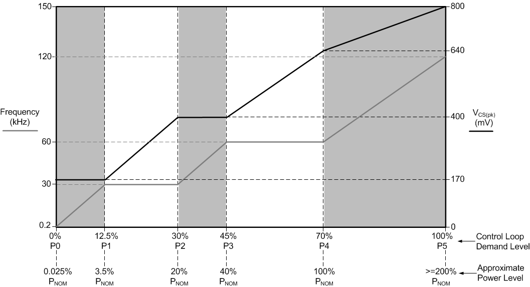
In the high-power region of the modulator, the device adjusts both peak current and frequency together, to allow higher power delivery with a modest increase in peak current. In this high-power region, the power stage typically transitions into continuous-conduction mode (CCM), particularly at low line. The combination of up to 2× frequency increase and 1.25× peak current increase in CCM allows up to 2× peak power delivery capability for a given transformer size. Figure 41 provides details regarding the modulator peak current (in mV at the CS pin) and switching frequency variation vs power demand level. The frequency adjusts from a minimum of 200 Hz up to a maximum of 120 kHz. The peak-current sense voltage at the CS pin varies from 172 mV to 800 mV. Table 6 summarizes the modulator breakpoints and corresponding percentage power levels.
 Figure 41. Modulator Modes and Frequency Variations with Power Level
 For no load and very light loads (P0 to P1 region) the modulator operates in a pulse frequency modulation (PFM) mode. In PFM mode, the device maintains a constant peak current in the transformer magnetizing inductance, so that the energy transferred in each switching cycle is fixed. The magnetic sensing, fixed-point sampling scheme requires that the device always imposes a minimum peak current. This minimum peak-current demand naturally results in a minimum transformer magnetizing volt-second product that the device maintains across the input line voltage range. Ensuring a minimum on-time magnetizing volt-seconds also ensures a balancing volt-second flyback interval, during which the device guarantees the availability of the output voltage sample. Magnetic Sensing: Power Stage Design Constraints outlines the transformer design constraints necessary to comply with the minimum on-time and minimum required volt-seconds.
In the P0 to P1 region, the energy transfer per switching cycle is maximized, which in turn minimizes the switching frequency and associated switching and drive losses, to improve efficiency. However, due to concerns about audible noise in this region, the peak current VCS(min) in this region is limited to 22% of the peak VCS(max) at the maximum demand level. This peak-current derating maintains the transformer peak flux density to 22% of the peak, to minimize transformer-induced audible noise. Assuming a maximum peak flux density of typically 300 mT at highest peak current, this derating sets the peak flux level at approximately 65 mT in the light-load region. Empirically, this flux level greatly reduces magnetic audible noise for a variety of power levels and transformer designs. In this region, the use of sleep modes (where most of the device internal blocks are powered down in between switching cycles) minimizes the controller power consumption. Minimizing controller power consumption helps reduce total standby power consumption, and also greatly eases the bias design constraints.
For higher loads above P1 (P1 to P2 region), the device fixes the modulator frequency at a low value above the audible range, while the peak switch current ramps up from the minimum level, to deliver the increased output power. Maintaining a fixed low-switching frequency while ramping peak current, minimizes switching losses to provide good light-load efficiency.
For higher loads above P2 (P2 to P3 region), the device maintains a constant peak-switch current, while the modulator frequency ramps to its nominal operating value. The normal heavy load (between 40% and 100% of rated) operating power range lies between P3 and P4. In this region the device maintains a constant switching frequency at the nominal value fSW(nom), and the peak switch current ramps to achieve increased output power. Fixed-frequency operation at nominal operating power results in consistent EMI and transient load step performance.
Table 6. Frequency and Peak-Current Modulator Operating Ranges and Breakpoints
| MODULATOR BREAKPOINT | DEMAND LEVEL (%) | APPROXIMATE POWER LEVEL % of PNOM | VCS PEAK | FREQUENCY fSW | ||
|---|---|---|---|---|---|---|
| (mV) | (kHz) | |||||
| PO0 | 0 | 0.025 | 172 | VCS(min) | 0.200 | fSW(min) |
| PO1 | 12.5 | 3.5 | 172 | VCS(min) | 30 | fSW(LL) |
| PO2 | 30 | 20 | 400 | VCS(nom) | 30 | fSW(LL) |
| PO3 | 45 | 40 | 400 | VCS(nom) | 60 | fSW(nom) |
| PO4 | 70 | 100 | 640 | VCS(bcm) | 60 | fSW(nom) |
| PO5 | 100 | > 200 | 800 | VCS(max) | 120 | fSW(max) |
The peak-power range lies between P4 and P5. In this region the transformer can operate in CCM depending on loading and line voltage. By increasing the frequency appropriately, higher average input current can be processed for the same peak current, so the transformer size does not need to increase substantially for a high-rated transient peak power. The modulator does, however, also increase the peak current in this region of operation, requiring a modest increase in transformer size, but this allows a larger transient peak power to be delivered. The modulator control loop adjusts both the frequency and peak current according to the power demand so that the increased frequency and peak current meets the load demand.
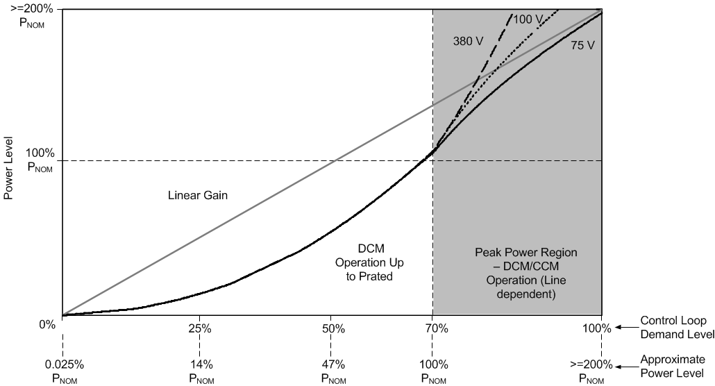
Figure 42 shows the modulator gain curve, specifically the non-linear modulator gain vs load. At very light loads, the modulator gain remains low, to help counteract the effect of the higher power stage gain as the load resistance increases. This low gain helps stabilize the magnetic regulation loop in the light load territory, where the output voltage sample rate drops with decreasing switching frequency. At heavier loads, the modulator gain progressively and smoothly increases to help improve transient response. When the switching frequency increases above the maximum magnetic sense sample rate (fSMP(max)), the magnetic sense voltage control sample rate is clamped.
 Figure 42. Modulator Gain Curves vs Bulk Capacitor Voltage