ZHCSD93A january   2015  – december 2020 UCC28700-Q1

PRODUCTION DATA  

  1.   1
  2. 特性
  3. 应用
  4. 说明
  5. Revision History
  6. Pin Configuration and Functions
    1. 5.1 Pin Functions
  7. Specifications
    1. 6.1 Absolute Maximum Ratings #GUID-6657BD5B-29CE-4F76-A6A3-BA4B57482A18/SLUSB418335
    2. 6.2 ESD Ratings
    3. 6.3 Recommended Operating Conditions
    4. 6.4 Thermal Information
    5. 6.5 Electrical Characteristics
    6. 6.6 Switching Characteristics
    7. 6.7 Typical Characteristics
  8. Detailed Description
    1. 7.1 Overview
    2. 7.2 Functional Block Diagram
    3. 7.3 Feature Description
      1. 7.3.1 Detailed Pin Description
        1. 7.3.1.1 VDD (Device Bias Voltage Supply)
        2. 7.3.1.2 GND (Ground)
        3. 7.3.1.3 VS (Voltage-Sense)
        4. 7.3.1.4 DRV (Gate Drive)
        5. 7.3.1.5 CS (Current Sense)
        6. 7.3.1.6 CBC (Cable Compensation)
      2. 7.3.2 Fault Protection
    4. 7.4 Device Functional Modes
      1. 7.4.1 Primary-Side Voltage Regulation
      2. 7.4.2 Primary-Side Current Regulation
      3. 7.4.3 Valley-Switching
      4. 7.4.4 Start-Up Operation
  9. Applications and Implementation
    1. 8.1 Application Information
    2. 8.2 Typical Application
      1. 8.2.1 Design Requirements
      2. 8.2.2 Detailed Design Procedure
        1. 8.2.2.1 Transformer Parameter Verification
        2. 8.2.2.2 Output Capacitance
        3. 8.2.2.3 VDD Capacitance, CDD
        4. 8.2.2.4 VDD Start-Up Resistance, RSTR
        5. 8.2.2.5 VS Resistor Divider, Line Compensation, and Cable Compensation
        6. 8.2.2.6 Input Bulk Capacitance and Minimum Bulk Voltage
        7. 8.2.2.7 Transformer Turns Ratio, Inductance, Primary-Peak Current
        8. 8.2.2.8 Standby Power Estimate
      3. 8.2.3 Application Curves
  10. Power Supply Recommendations
  11. 10Layout
    1. 10.1 Layout Guidelines
    2. 10.2 Layout Example
  12. 11Device and Documentation Support
    1. 11.1 Device Support
      1. 11.1.1 Device Nomenclature
        1. 11.1.1.1  Capacitance Terms in Farads
        2. 11.1.1.2  Duty Cycle Terms
        3. 11.1.1.3  Frequency Terms in Hertz
        4. 11.1.1.4  Current Terms in Amperes
        5. 11.1.1.5  Current and Voltage Scaling Terms
        6. 11.1.1.6  Transformer Terms
        7. 11.1.1.7  Power Terms in Watts
        8. 11.1.1.8  Resistance Terms in Ω
        9. 11.1.1.9  Timing Terms in Seconds
        10. 11.1.1.10 Voltage Terms in Volts
        11. 11.1.1.11 AC Voltage Terms in VRMS
        12. 11.1.1.12 Efficiency Terms
    2. 11.2 Documentation Support
      1. 11.2.1 Related Documentation
    3. 11.3 Trademarks
  13.   Mechanical, Packaging, and Orderable Information

封装选项

机械数据 (封装 | 引脚)
散热焊盘机械数据 (封装 | 引脚)
订购信息

Application Curves

GUID-C31455D5-7EE4-4E83-A134-CAD160F0BBE7-low.png
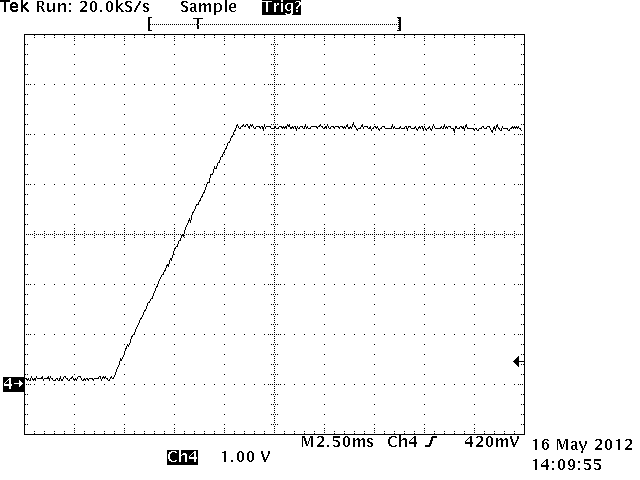
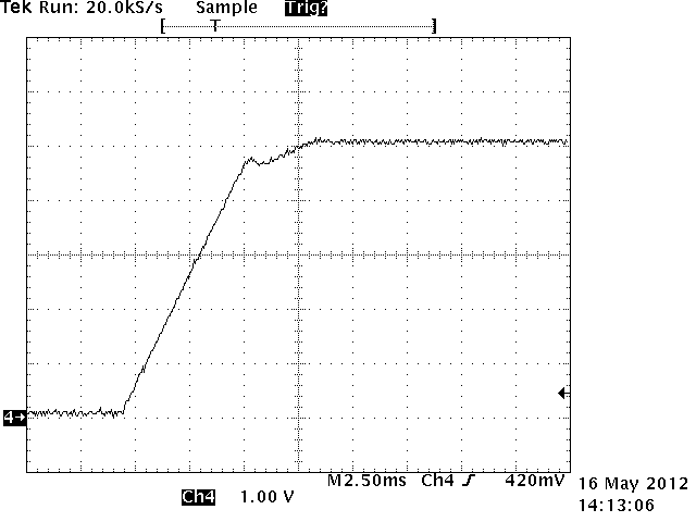
Figure 8-2 Output at Startup at 115-V RMS (No Load)
GUID-53DAD914-F7B3-4F31-AA0A-CB32B6F9EEF6-low.png
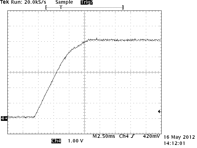
Figure 8-4 Output at Startup at 230-V RMS (No Load)
GUID-68602206-F036-4C59-970D-48DA2E95A969-low.png
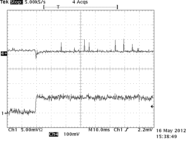
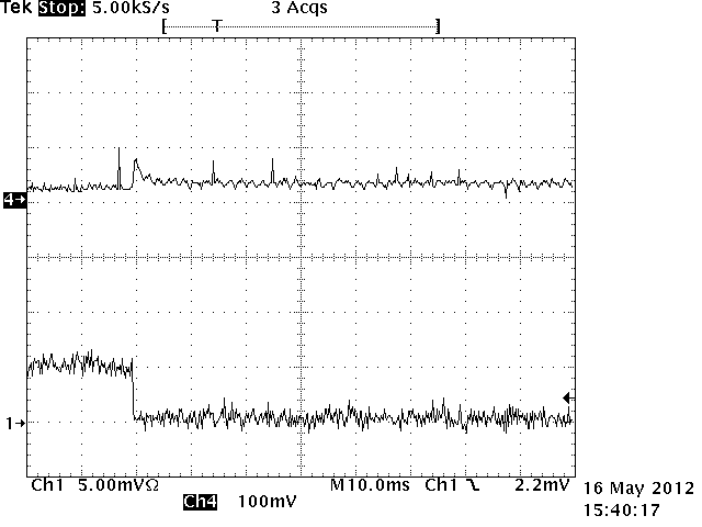
CH1 = IO, CH4 = VO With a 5-V Offset
Figure 8-6 Load Transients: (0.1-A to 0.6-A Load Step)
GUID-51737FC2-DA8C-40F2-9520-03CB61F98758-low.png
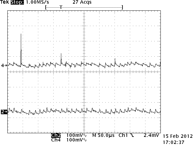
CH4 = VO, Output voltage at EVM output
CH2 = VO, Output voltage measured at the end of the 3M of cable in parallel with a 1-uF capacitor. The output voltage has less than 50 mV of output ripple at the end of the cable.
Figure 8-8 Output Ripple Voltage at Full Load
GUID-A86DDE7B-C818-48DD-905E-7AB805ACFCE9-low.png
Figure 8-3 Output at Startup at 115-V RMS (5-Ω Load)
GUID-F5A7B132-CA53-45D5-98CF-0276E8AC0959-low.png
Figure 8-5 Output at Startup at 230-V RMS (5-Ω Load)
GUID-F702BC46-E973-41BD-833B-76A135F0CE78-low.png
CH1 = IO, CH4 = VO With a 5-V Offset
Figure 8-7 Load Transients: (0.6-A to 0.1-A Load Step)