ZHCSAH7C November 2012 – June 2017 UCC28710 , UCC28711 , UCC28712 , UCC28713
PRODUCTION DATA.
- 1 特性
- 2 应用
- 3 说明
- 4 修订历史记录
- 5 Device Comparison Table
- 6 Pin Configuration and Functions
- 7 Specifications
- 8 Detailed Description
-
9 Application and Implementation
- 9.1 Application Information
- 9.2
Typical Application
- 9.2.1 Design Requirements
- 9.2.2
Detailed Design Procedure
- 9.2.2.1 Custom Design With WEBENCH® Tools
- 9.2.2.2 Stand-by Power Estimate
- 9.2.2.3 Input Bulk Capacitance and Minimum Bulk Voltage
- 9.2.2.4 Transformer Turns Ratio, Inductance, Primary-Peak Current
- 9.2.2.5 Transformer Parameter Verification
- 9.2.2.6 Output Capacitance
- 9.2.2.7 VDD Capacitance, CDD
- 9.2.2.8 VS Resistor Divider, Line Compensation, and Cable Compensation
- 9.2.3 Application Curves
- 10Power Supply Recommendations
- 11Layout
- 12器件和文档支持
- 13机械、封装和可订购信息
11 Layout
11.1 Layout Guidelines
- High frequency bypass Capacitor C5 should be placed across Pin 1 and 4 as close as you can get it to the pins.
- Resistor R4 and C5 form a low pass filter and the connection of R4 and C5 should be as close to the VDD pin as possible.
- The VS pin controls the output voltage through the transformer turns ratio and the voltage divider of R5 and R11. Note the trace length between the R5, R11 and VS pin should be as short as possible to reduce or eliminate possible EMI coupling.
- Note the IC ground and power ground should meet at the bulk capacitor’s (C6 and C7) return. Try to ensure that high frequency/high current from the power stage does not go through the signal ground.
- The high frequency/high current path that you need to be cautious of on the primary is C7 +, T1 (P5, P3), Q1d, Q1s, R8 to the return of C6 and C7. Try to keep all high current loops as short as possible.
- Try to keep all high current loops as short as possible.
- Keep all high current/high frequency traces away from or perpendicular to other traces in the design.
- Traces on the voltage clamp formed by D1, R2, D3 and C2 as short as possible.
- C6 return needs to be as close to the bulk capacitor supply as possible. This reduces the magnitude of dv/dt caused by large di/dt.
- Avoid mounting semiconductors under magnetics.

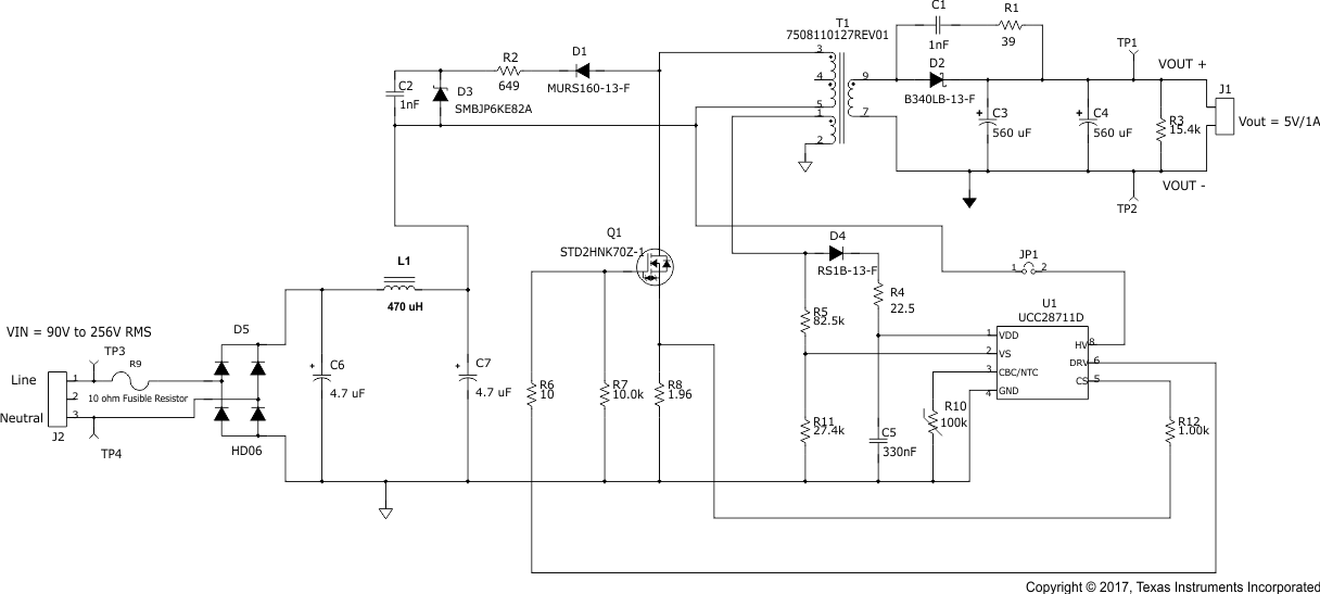
No value means not populated.
Figure 29. 5-W USB Adapter Schematic
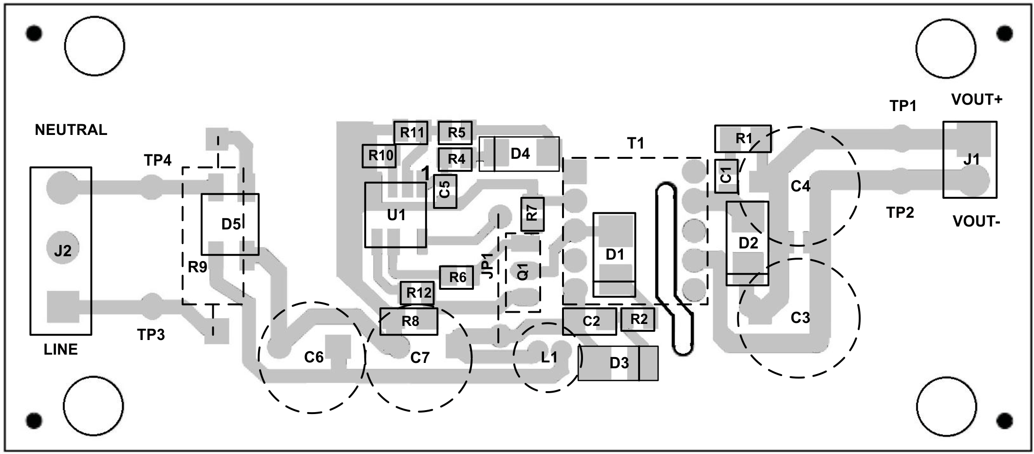
11.2 Layout Example
 Figure 30. Layout Example Schematic