ZHCSAH7C November 2012 – June 2017 UCC28710 , UCC28711 , UCC28712 , UCC28713
PRODUCTION DATA.
- 1 特性
- 2 应用
- 3 说明
- 4 修订历史记录
- 5 Device Comparison Table
- 6 Pin Configuration and Functions
- 7 Specifications
- 8 Detailed Description
-
9 Application and Implementation
- 9.1 Application Information
- 9.2
Typical Application
- 9.2.1 Design Requirements
- 9.2.2
Detailed Design Procedure
- 9.2.2.1 Custom Design With WEBENCH® Tools
- 9.2.2.2 Stand-by Power Estimate
- 9.2.2.3 Input Bulk Capacitance and Minimum Bulk Voltage
- 9.2.2.4 Transformer Turns Ratio, Inductance, Primary-Peak Current
- 9.2.2.5 Transformer Parameter Verification
- 9.2.2.6 Output Capacitance
- 9.2.2.7 VDD Capacitance, CDD
- 9.2.2.8 VS Resistor Divider, Line Compensation, and Cable Compensation
- 9.2.3 Application Curves
- 10Power Supply Recommendations
- 11Layout
- 12器件和文档支持
- 13机械、封装和可订购信息
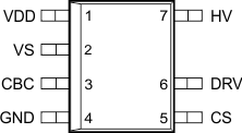
6 Pin Configuration and Functions
UCC28710 D Package
7-Pin SOIC
Top View

UCC28711, UCC28712, UCC28713 D Package
7-Pin SOIC
Top View

Pin Functions
| PIN | I/O | DESCRIPTION | ||
|---|---|---|---|---|
| NAME | UCC28710 | UCC28711 UCC28712 UCC28713 |
||
| CBC | 3 | — | I | Cable compensation is a programming pin for compensation of cable voltage drop. Cable compensation is programmed with a resistor to GND. |
| CS | 5 | 5 | I | Current sense input connects to a ground-referenced current-sense resistor in series with the power switch. The resulting voltage is used to monitor and control the peak primary current. A series resistor can be added to this pin to compensate the peak switch current levels as the AC-mains input varies. |
| DRV | 6 | 6 | O | Drive is an output used to drive the gate of an external high voltage MOSFET switching transistor. |
| GND | 4 | 4 | — | The ground pin is both the reference pin for the controller and the low-side return for the drive output. Special care should be taken to return all AC decoupling capacitors as close as possible to this pin and avoid any common trace length with analog signal return paths. |
| HV | 7 | 7 | I | The high-voltage pin connects directly to the rectified bulk voltage and provides charge to the VDD capacitor for start-up of the power supply. |
| NTC | — | 3 | I | NTC an interface to an external negative temperature coefficient resistor for remote temperature sensing. Pulling this pin low shuts down PWM action. |
| VDD | 1 | 1 | I | VDD is the bias supply input pin to the controller. A carefully-placed bypass capacitor to GND is required on this pin. |
| VS | 2 | 2 | I | Voltage sense is an input used to provide voltage and timing feedback to the controller. This pin is connected to a voltage divider between an auxiliary winding and GND. The value of the upper resistor of this divider is used to program the AC-mains run and stop thresholds and line compensation at the CS pin. |