ZHCSEK1B December 2013 – October 2015 UCC28722
PRODUCTION DATA.
- 1 特性
- 2 应用
- 3 说明
- 4 修订历史记录
- 5 Pin Configuration and Functions
- 6 Specifications
- 7 Detailed Description
-
8 Application and Implementation
- 8.1 Application Information
- 8.2
Typical Application
- 8.2.1 Design Requirements
- 8.2.2
Detailed Design Procedure
- 8.2.2.1 Stand-by Power Estimate
- 8.2.2.2 Input Bulk Capacitance and Minimum Bulk Voltage
- 8.2.2.3 Transformer Turns Ratio, Inductance, Primary-Peak Current
- 8.2.2.4 Transformer Parameter Verification
- 8.2.2.5 Output Capacitance
- 8.2.2.6 VDD Capacitance, CDD
- 8.2.2.7 VS Resistor Divider, Line Compensation, and Cable Compensation
- 8.2.2.8 Startup Resistance and Startup Time
- 8.2.3 Application Curves
- 9 Power Supply Recommendations
- 10Layout
- 11器件和文档支持
- 12机械、封装和可订购信息
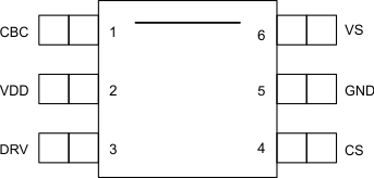
5 Pin Configuration and Functions
DBV Package
6-Pin SOT-23
Top View

Pin Functions
| PIN | I/O | DESCRIPTION | |
|---|---|---|---|
| NAME | NO. | ||
| CBC | 1 | I | Cable compensation is a programming pin for compensation of cable voltage drop. Cable compensation is programmed with a resistor to GND. |
| CS | 4 | I | Current sense input connects to a ground-referenced current-sense resistor in series with the power switch. The resulting voltage is used to monitor and control the peak primary current. A series resistor can be added to this pin to compensate the peak switch current levels as the AC-mains input varies. |
| DRV | 3 | O | Drive is an output used to drive the base of an external high voltage NPN transistor. |
| GND | 5 | — | The ground pin is both the reference pin for the controller and the low-side return for the drive output. Special care should be taken to return all AC decoupling capacitors as close as possible to this pin and avoid any common trace length with analog signal return paths. |
| VDD | 2 | I | VDD is the bias supply input pin to the controller. A carefully-placed bypass capacitor to GND is required on this pin. |
| VS | 6 | I | Voltage sense is an input used to provide voltage and timing feedback to the controller. This pin is connected to a voltage divider between an auxiliary winding and GND. The value of the upper resistor of this divider is used to program the AC-mains run and stop thresholds and line compensation at the CS pin. |