ZHCSGD9 June 2017 UCC28730-Q1
PRODUCTION DATA.
- 1 特性
- 2 应用
- 3 说明
- 4 修订历史记录
- 5 Pin Configuration and Functions
- 6 Specifications
-
7 Detailed Description
- 7.1 Overview
- 7.2 Functional Block Diagram
- 7.3 Feature Description
- 7.4 Device Functional Modes
-
8 Application and Implementation
- 8.1 Application Information
- 8.2
Typical Application
- 8.2.1 Design Requirements
- 8.2.2
Detailed Design Procedure
- 8.2.2.1 Stand-By Power Estimate
- 8.2.2.2 Input Bulk Capacitance and Minimum Bulk Voltage
- 8.2.2.3 Transformer Turns Ratio, Inductance, Primary-Peak Current
- 8.2.2.4 Transformer Parameter Verification
- 8.2.2.5 Output Capacitance
- 8.2.2.6 VDD Capacitance, CVDD
- 8.2.2.7 VS Resistor Divider, Line Compensation, and Cable Compensation
- 8.2.2.8 VS Wake-Up Detection
- 8.2.3 Application Curves
- 8.3 Do's and Don'ts
- 9 Power Supply Recommendations
- 10Layout
- 11器件和文档支持
- 12机械、封装和可订购信息
8 Application and Implementation
NOTE
Information in the following applications sections is not part of the TI component specification, and TI does not warrant its accuracy or completeness. TI’s customers are responsible for determining suitability of components for their purposes. Customers should validate and test their design implementation to confirm system functionality.
8.1 Application Information
The UCC28730-Q1 device is a PSR controller optimized for isolated-flyback AC-to-DC single-output supply applications in the 5-W to 25-W range, providing constant-voltage (CV) mode control and constant current (CC) mode control for precise output regulation. Higher-power, multiple-output applications and other variations may also be supported. It is capable of switching at a very low frequency to facilitate achieving stand-by input power consumption of less than 5 mW.
To maintain fast transient response at such low-switching frequencies, the device recognizes a wake-up signal at the VS input generated by a companion device, the secondary-side voltage monitor UCC24650.
8.2 Typical Application
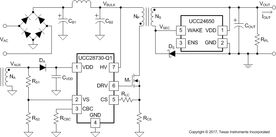
A typical application for the UCC28730-Q1 includes the compatible UCC24650 Wake-Up Monitor device to regulate an isolated low-voltage DC output with low output capacitance. When the UCC28730-Q1 is operating in the low-frequency Wait state, the UCC24650 alerts the UCC28730-Q1 to a sudden load increase, avoiding the need for extremely high output capacitance to hold up between power cycles. As shown in Figure 23, the output rectification uses a ground-referenced diode to facilitate application of the UCC24650. A ground-referenced synchronous rectifier may also be used.
NOTE
This figure is simplified to illustrate the basic application of the UCC28730-Q1 and does not show all of the components and networks needed for an actual converter design, nor all of the possible circuit variations.
 Figure 23. Simplified Application With Ground-Referenced Diode
8.2.1 Design Requirements
The following table illustrates a typical subset of high-level design requirements for a particular converter, of which many of the parameter values are used in the various design equations in this section.
Table 1. Design Example Performance Requirements
| PARAMETER | CONDITIONS | MIN | NOM | MAX | UNITS | |
|---|---|---|---|---|---|---|
| VIN | AC-Line Input Voltage | 85 | 115 / 230 | 264 | VRMS | |
| fLINE | Line Frequency | 47 | 50 / 60 | 63 | Hz | |
| VOCV | Output Voltage, CV Mode | VIN(min) ≤ VIN ≤ VIN(max), IOUT ≤ IOCC | 4.75 | 5.0 | 5.25 | V |
| IOCC | Output Current, CC Mode | VIN(min) ≤ VIN ≤ VIN(max), IOUT = IOCC | 2.0 | 2.1 | 2.2 | A |
| VRIPPLE | Output Voltage Ripple | VIN(min) ≤ VIN ≤ VIN(max), IOUT ≤ IOCC | 80 | mVpp | ||
| Output Over-Voltage Limit | 5.6 | V | ||||
| Output Over-Current Limit | 2.1 | A | ||||
| VIN(run) | Start-Up Input Voltage | IOUT = IOCC | 72 | VRMS | ||
| VOCC | Minimum Output Voltage, CC Mode | IOUT = IOCC | 2 | V | ||
| ηAVG | Average Efficiency | Average of 25%, 50%, 75% 100% Load, at VIN = 115 VRMS and 230 VRMS | 80% | |||
| η10 | Light-Load Efficiency | At 10 % Load, at VIN = 115 VRMS and 230 VRMS | 75% | |||
| PSTBY | Stand-by Input Power Consumption | At VIN = 115 VRMS and 230 VRMS | 4.5 | mW | ||
Many other necessary design parameters, such as fMAX and VBULK(min) for example, may not be listed in such a table. These values may be selected based on design experience or other considerations, and may be iterated to obtain optimal results.
8.2.2 Detailed Design Procedure
This procedure outlines the steps to design a constant-voltage, constant-current flyback converter using the UCC28730-Q1 controller. Refer to Figure 23 for component names and network locations. The design procedure equations use terms that are defined below. The primary-side and secondary-side snubbers or clamps are not designed in this procedure.
8.2.2.1 Stand-By Power Estimate
The extra-low operating frequency capability and minimal bias power of the UCC28730-Q1, in conjunction with its companion micro-power wake-up device UCC24650, allow for the achievement of less than 5-mW input stand-by power consumption under no-load conditions. This is often referred to as zero-power stand-by.
Assuming that no-load stand-by power is a critical design parameter, determine the estimated no-load input power based on the target maximum switching frequency and the maximum output power. The following equation estimates the stand-by power of the converter.

For a typical flyback converter, ηSB may range between 0.5 and 0.7, but the lower factor should be used for an initial estimate. Also, fMIN should be estimated at 3x to 4x fSW(min) to allow for possible parameter adjustment.
If the PSTBY calculation result is well below 5 mW, there is an excellent chance of achieving zero-power stand-by in the actual converter. If the result is near 5 mW, some design adjustment to fMAX, fMIN, and ηSB may be needed to achieve zero-power. If the result is well above 5 mW, there is little chance to achieve zero-power at the target power level unless additional special circuitry and design effort is applied.
8.2.2.2 Input Bulk Capacitance and Minimum Bulk Voltage
Bulk capacitance may consist of one or more capacitors connected in parallel, often with some inductance between them to suppress differential-mode conducted noise. EMI filter design is beyond the scope of this procedure.
Determine the minimum voltage on the input capacitance, CB1 and CB2 total, in order to determine the maximum NP to NS turns ratio of the transformer. The input power of the converter based on target full-load efficiency, minimum input RMS voltage, and minimum AC input frequency are used to determine the input capacitance value.
Maximum input power is used in the CBULK calculation and is determined by the VOCV, IOCC, and full-load efficiency targets.

The below equation provides an accurate solution for input capacitance needed to achieve a minimum bulk valley voltage target VBULK(min), accounting for hold-up during any loss of AC power for a certain number of half-cycles, NHC, by an AC-line drop-out condition. Alternatively, if a given input capacitance value is prescribed, iterate the VBULK(min) value until that target capacitance is obtained, which determines the VBULK(min) expected for that capacitance.

8.2.2.3 Transformer Turns Ratio, Inductance, Primary-Peak Current
The maximum primary-to-secondary turns ratio can be determined by the target maximum switching frequency at full load, the minimum input capacitor bulk voltage, and the estimated DCM quasi-resonant time.
First, determine the maximum duty cycle of the MOSFET based on the target maximum switching frequency, fMAX, the secondary conduction duty cycle, DMAGCC, and the DCM resonant period, tR. For tR, assume 2 µs (500-kHz resonant frequency), if you do not have an estimate from experience or previous designs. For the transition mode operation limit, the time interval from the end of the secondary current conduction to the first resonant valley of the VDS voltage is ½ of the DCM resonant period, or 1 µs assuming 500 kHz. Actual designs vary. DMAX can be determined using the equation below.

DMAGCC is defined as the secondary diode conduction duty cycle during constant current, CC, operation. In the UCC28730-Q1, it is fixed internally at 0.432. Once DMAX is known, the ideal turns ratio of the primary-to-secondary windings can be determined with the equation below. The total voltage on the secondary winding needs to be determined, which is the total of VOCV, the secondary rectifier drop VF, and cable compensation voltage VOCBC, if used. For 5-V USB charger applications, for example, a turns ratio in the range of 13 to 15 is typically used.

The actual turns ratio depends on the actual number of turns on each of the transformer windings. Choosing NPS > NPS(ideal) results in an output power limit lower than (VOCV x IOCC) when operating at VIN(min), and line-frequency ripple may appear on VOUT. Choosing NPS < NPS(ideal) allows full-power regulation down to VIN(min), but increases conduction losses and the reverse voltage stress on the output rectifier.
Once the actual turns ratio is determined from a detailed transformer design, use this ratio for the following parameter calculations.
The UCC28730-Q1 constant-current regulation is achieved by maintaining a maximum DMAGCC duty cycle of 0.432 at the maximum primary current setting. The transformer turns ratio and constant-current regulating factor determine the current-sense resistor, RCS, for a regulated constant-current target, IOCC. Actual implementation of RCS may consist of multiple parallel resistors to meet power rating and accuracy requirements.
Since not all of the energy stored in the transformer is transferred to the secondary output, a transformer efficiency term, ηXFMR, is used to account for the core and winding loss ratio, leakage inductance loss ratio, and primary bias power ratio with respect to the rated output power. At full load, an overall transformer efficiency estimate of 0.91, for example, includes ~3% leakage inductance loss, ~5% core and winding loss, and ~1% bias power. Actual loss ratios may vary from this example.

The primary-transformer inductance can be calculated using the standard energy storage equation for flyback transformers. Primary current, maximum switching frequency and output and transformer power losses are included in the equation below.
Initially, determine the transformer peak primary current, IPP(max).
Peak-primary current is simply the maximum current-sense threshold divided by the current-sense resistance.

Then, calculate the primary inductance of the transformer, LP.

The auxiliary winding to secondary winding turns ratio, NAS, is determined by the lowest target operating output voltage in constant current regulation, the VDD turn-off threshold of the UCC28730-Q1, and the forward diode drops in the respective winding networks.

There is additional energy supplied to VDD from the transformer leakage inductance energy which may allow a lower turns ratio to be used in many designs.
8.2.2.4 Transformer Parameter Verification
The transformer turns ratio selected affects the MOSFET VDS and secondary rectifier reverse voltage VREV, these should be reviewed.
The secondary rectifier reverse voltage stress is determined by the equation below. A snubber around the rectifier may be necessary to suppress any voltage spike, due to secondary leakage inductance, which adds to VREV.

For the MOSFET VDS peak stress, an estimated leakage inductance voltage spike, VLK, should to be included.

In the high-line, minimum-load condition, the UCC28730-Q1 requires a minimum on-time of the MOSFET (tON(min)) and minimum demagnetization time of the secondary rectifier (tDMAG(min)). The selection of fMAX, LP and RCS affects the actual minimum tON and tDMAG achieved. The following equations are used to determine if the minimum tON is greater than tCSLEB and minimum tDMAG target of >1.2 µs is achieved.


8.2.2.5 Output Capacitance
With ordinary flyback converters, the output capacitance value is typically determined by the transient response requirement for a specific load step, ITRAN, sometimes from a no-load condition. For example, in some USB charger applications, there is requirement to maintain a transient minimum VO of 4.1 V with a load-step of 0 mA to 500 mA. Equation 20 below assumes that the switching frequency can be at the UCC28730-Q1 minimum of fSW(min).

This results in a COUT value of over 17,000 µF, unless a substantial pre-load is used to raise the minimum switching frequency. However, the wake-up feature allows the use of a much smaller value for COUT because the wake-up response immediately cancels the Wait state and provides high-frequency power cycles to recover the output voltage from the load transient. The secondary-side voltage monitor UCC24650 provides the UCC28730-Q1 with a wake-up signal when it detects a -3% droop in output voltage.

where
- (dVOUT/dt) is the slope at which the UCC24650 must detect the VOUT droop. Use a slope factor of 3700 V/s or lower for this calculation.
The UCC28730-Q1 incorporates internal voltage-loop compensation circuits so that external compensation is not necessary, provided that the value of COUT is high enough. The following equation determines a minimum value of COUT necessary to maintain a phase margin of about 40 degrees over the full-load range. KCo is a dimensionless factor which has a value of 100.

Another consideration for selecting the output capacitor(s) is the maximum ripple voltage requirement, VRIPPLE(max), which is reviewed based on the maximum output load, the secondary-peak current, and the equivalent series resistance (ESR) of the capacitor. The two major contributors to the output ripple voltage are the change in VOUT due to the charge and discharge of COUT between each switching cycle and the step in VOUT due to the ESR of COUT. TI recommends an initial allocation of 33% of VRIPPLE(max) to ESR, 33% to COUT, and the remaining 33% to account for additional low-level ripple from EMI-dithering, valley-hopping, sampling noise and other random contributors. In Equation 23, a margin of 50% is applied to the capacitor ESR requirement to allow for aging. In Equation 24, set ΔVCQ = 0.33 x VRIPPLE(max) to determine the minimum value of COUT with regard to ripple voltage limitation. If other allocations of the allowable ripple voltage are desired, these equations may be adjusted accordingly.


Choose the largest value of the previous COUT calculations for the minimum output capacitance. If the value of COUT becomes excessive to meet a stringent ripple limitation, a C-L-C pi-filter arrangement can be considered to as an alternative to a simple capacitor-only filter. This arrangement is beyond the scope of this datasheet.
8.2.2.6 VDD Capacitance, CVDD
A capacitor is required on VDD to provide:
- Run-state bias current during start-up while VDD falls toward UVLO, until VOCC is reached,
- Wait-state bias current between steady-state low-frequency power cycles and
- Wait-state bias current between minimum-frequency power cycles while VOUT recovers from a transient overshoot.
Generally, the value to satisfy (3) also satisfies (2) and (1), however the value for (1) may be the largest if the converter must provide high output current at a voltage below VOCC during power up.
The capacitance on VDD needs to supply the device operating current until the output of the converter reaches the target minimum operating voltage in constant-current regulation, VOCC. At that point, the auxiliary winding can sustain the bias voltage to the UCC28730-Q1 above the UVLO shutdown threshold. The total current available to charge the output capacitors and supply an output load and is the constant-current regulation target, IOCC.
Equation 25 assumes that all of the output current of the flyback is available to charge the output capacitance until the minimum output voltage is achieved. For margin, there is an estimated 1 mA of average gate-drive current added to the run current and 1 V added to the minimum VDD.

At light loads, the UCC28730-Q1 enters a Wait-state between power cycles to minimize bias power and improve efficiency. Equation 26 estimates the minimum capacitance needed to obtain a target maximum ripple voltage on VDD (VVDD(maxΔ) < 1 V, for example) during the Wait state, which occurs at the lowest possible switching frequency.

Choose the largest value of the previous CVDD calculations for the minimum VDD capacitance.
8.2.2.7 VS Resistor Divider, Line Compensation, and Cable Compensation
The VS divider resistors determine the output voltage regulation point of the flyback converter. Also, the high-side divider resistor, RS1, determines the line voltage at which the controller enables continuous DRV operation. RS1 is initially determined based on the transformer primary to auxiliary turns ratio and the desired input voltage operating threshold.

The low-side VS divider resistor, RS2, is selected based on the desired constant-voltage output regulation target, VOCV.

The UCC28730-Q1 can maintain tight constant-current regulation over input line by utilizing the line compensation feature. The line compensation resistor value, RLC, is determined by various system parameters and the combined gate-drive turn-off and MOSFET turn-off delays, tD. Assume a 50-ns internal propagation delay in the UCC28730-Q1.

The UCC28730-Q1 provides adjustable cable compensation of up to approximately +8% of VOCV by connecting a resistor between the CBC terminal and GND. This compensation voltage, VOCBC, represents the incremental increase in voltage, above the nominal no-load output voltage, needed to cancel or reduce the incremental decrease in voltage at the end of a cable due to its resistance. The programming resistance required for the desired cable compensation level at the converter output terminals can be determined using the equation below. As the load current changes, the cable compensation voltage also changes slowly to avoid disrupting control of the main output voltage. A sudden change in load current will induce a step change of output voltage at the end of the cable until the compensation voltage adjusts to the required level. Note that the cable compensation does not change the overvoltage protection (OVP) threshold,VOVP (see Electrical Characteristics), so the operating margin to OVP is less when cable compensation is used. If cable compensation is not required, CBC may remain unconnected.

8.2.2.8 VS Wake-Up Detection
The amplitude of the wake-up signal at the VS input must be high enough to be detected. This signal, which originates on the secondary winding, is limited by the impedances of the wake-up signal driver and the L-C resonant tank of the transformer windings. The signal is further attenuated by the VS divider resistors. To maximize the wake-up signal amplitude, the pulse width, tWAKE, of the wake-up signal should be at least 1/4-wavelength of the switched-node resonant frequency, fRES. The resonant frequency depends on the primary magnetizing inductance and the total equivalent capacitance at the switching node, that is, the primary-side MOSFET drain node. The switched-node capacitance, CSWN, includes the MOSFET COSS, the transformer winding capacitance, and all other stray circuit capacitance attached to the MOSFET drain. Use Equation 31 to determine fRES. Conversely, if fRES is known by experience or measurement, CSWN can be derived from Equation 31.

Since the wake-up pulse width is typically fixed by the driver device, such as the UCC24650, maximum signal strength is obtained when Equation 32 is true. Since LP is generally fixed by other system requirements, only CSWN can be reduced to increase fRES, if necessary.

Equation 33 is used to ensure that there is sufficient amplitude at the VS input to reliably trigger the wake-up function, where RWAKE_TOT is the total secondary-side resistance of the wake-up signal driver and any series resistance. An over-drive of 15 mV is added to the wake-up threshold level for margin.

8.2.3 Application Curves
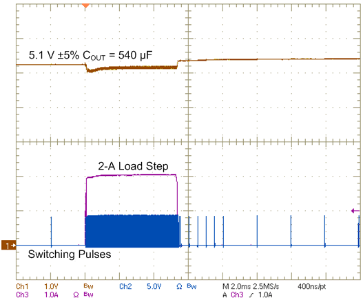
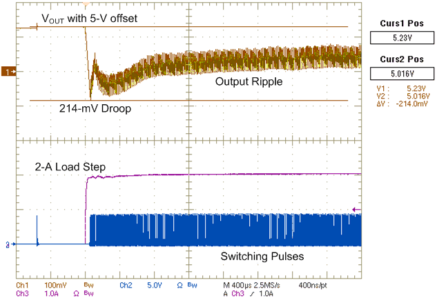
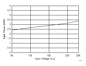
The following figures indicate the transient response of a 5-V, 10-W flyback converter which receives a pulsed step-load of 2 A while operating in the no-load stand-by condition. Figure 27 indicates the no-load stand-by input power consumption achieved by this converter over the full AC input range. Zero-Power operation is achieved while retaining fast transient response to a full load step.
 Figure 24. 2-A Load Step During Stand-by Operation
 Figure 26. Wake-Up Pulse Triggering Response from UCC28730-Q1 Primary-Side Controller


8.3 Do's and Don'ts
- During no-load operation, do allow sufficient margin for variations in VDD level to avoid the UVLO shutdown threshold. Also, at no-load, keep the average switching frequency, <fSW>, greater than 2 x fSW(min) to avoid a rise in output voltage.
- Do clean flux residue and contaminants from the PCB after assembly. Uncontrolled leakage current from VS to GND causes the output voltage to increase, while leakage current from HV or VDD to VS causes output voltage to decrease.
- If ceramic capacitors are used for VDD, do use quality parts with X7R or X5R dielectric rated 50 V or higher to minimize reduction of capacitance due to dc-bias voltage and temperature variation.
- Do not use leaky components if less than 5-mW stand-by input power consumption is a design requirement.
- Do not probe the VS node with an ordinary oscilloscope probe; the probe capacitance can alter the signal and disrupt regulation. Do observe VS indirectly by probing the auxiliary winding voltage at RS1 and scaling the waveform by the VS divider ratio.