ZHCSH21A October 2017 – February 2018 UCC28780
PRODUCTION DATA.
- 1 特性
- 2 应用
- 3 说明
- 4 修订历史记录
- 5 Pin Configuration and Functions
- 6 Specifications
-
7 Detailed Description
- 7.1 Overview
- 7.2 Functional Block Diagram
- 7.3
Detailed Pin Description
- 7.3.1 BUR Pin (Programmable Burst Mode)
- 7.3.2 FB Pin (Feedback Pin)
- 7.3.3 VDD Pin (Device Bias Supply)
- 7.3.4 REF Pin (Internal 5-V Bias)
- 7.3.5 HVG and SWS Pins
- 7.3.6 RTZ Pin (Sets Delay for Transition Time to Zero)
- 7.3.7 RDM Pin (Sets Synthesized Demagnetization Time for ZVS Tuning)
- 7.3.8 RUN Pin (Driver Enable Pin)
- 7.3.9 SET Pin
- 7.4
Device Functional Modes
- 7.4.1 Adaptive ZVS Control with Auto-Tuning
- 7.4.2 Dead-Time Optimization
- 7.4.3 Control Law across Entire Load Range
- 7.4.4 Adaptive Amplitude Modulation (AAM)
- 7.4.5 Adaptive Burst Mode (ABM)
- 7.4.6 Low Power Mode (LPM)
- 7.4.7 Standby Power Mode (SBP)
- 7.4.8 Startup Sequence
- 7.4.9 Survival Mode of VDD
- 7.4.10 System Fault Protections
- 7.4.11 Pin Open/Short Protections
-
8 Application and Implementation
- 8.1 Application Information
- 8.2
Typical Application Circuit
- 8.2.1 Design Requirements
- 8.2.2 Detailed Design Procedure
- 8.2.3 Application Curves
- 9 Power Supply Recommendations
- 10Layout
- 11器件和文档支持
- 12机械、封装和可订购信息
封装选项
请参考 PDF 数据表获取器件具体的封装图。
机械数据 (封装 | 引脚)
- D|16
- RTE|16
散热焊盘机械数据 (封装 | 引脚)
- RTE|16
订购信息
7.3.5 HVG and SWS Pins
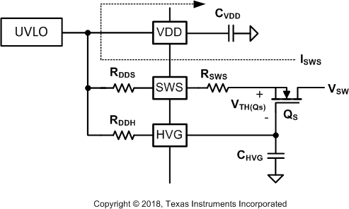
The HVG pin provides a controlled voltage to the gate of the depletion-mode MOSFET (QS), enabling QS to serve both VVDD startup and lossless ZVS sensing from the high-voltage switch node (VSW). During VVDD startup, the UVLO circuit commands two power-path switches connecting SWS and HVG pins to VDD pin with two internal current-limit resistors (RDDS and RDDH) separately, as shown in Figure 16. In this configuration, QS behaves as a current source to charge the VDD capacitor (CVDD). RDDS is set at 12 kΩ when VVDD is below 1 V to limit the maximum fault current under VDD pin short events. RDDS is reduced to 1 kΩ when VVDD rises above 1 V to allow VVDD to charge faster. The maximum charge current (ISWS) is affected by RDDS, the external series resistance (RSWS) from SWS pin to QS, and the threshold voltage of QS (VTH(Qs)). ISWS can be calculated as

 Figure 16. Operation of the VDD Startup Circuit
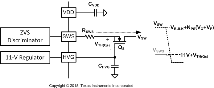
After VVDD reaches VVDD(ON), the two power-path switches open the connections among SWS, HVG, and VDD pins. At this point, a third power-path switch connects an internal 11-V regulator to the HVG pin for configuring QS to perform lossless ZVS sensing. As QS gate is fixed at 11 V and the drain pin voltage of QS becomes higher than the sum of QS threshold voltage (VTH(Qs)) and the 11-V gate voltage, QS turns off and the source pin voltage of QS can no longer follow the drain pin voltage change, so this gate control method makes QS act as a high-voltage blocking device with the drain pin connected to VSW. When the controller is switching, VSW can be lower than 11 V, so QS turns on and forces the source pin voltage to follow VSW, becoming a replica of the VSW waveform at the lower voltage level, as illustrated in Figure 17.
The limited window for monitoring the VSW waveform suffices for ZVS control of the UCC28780, since the ZVS tuning threshold (VTH(SWS)) is lower than that, which is at 9 V for VSET = 5 V and at 4 V for VSET = 0 V. The 9-V threshold is the auto-tuning target of the internal adaptive ZVS control loop for realizing a partial ZVS condition on the ACF using Si primary switches. On the other hand, performing full ZVS operation is more suitable for the ACF with GaN primary switches. The 4-V threshold can help to better compensate sensing delay between VSW and the SWS pin more than using a 0-V threshold. The internal 11-V regulator requires a high quality ceramic bypass capacitor (CHVG) between the HVG pin and GND for noise filtering and providing compensation to the regulator circuitry. The minimum CHVG value is 2.2 nF and an X7R-type dielectric capacitor is recommended. The controller enters a fault state if the HVG pin is open or shorted to GND during VVDD start-up, or if VHVG overshoot is higher than VHVG(OV) of 13.8 V in run state. The output short current of HVG regulator (IS(HVG)) is self-limited to around 1mA.
 Figure 17. ZVS Sensing by Reusing the VDD Startup Circuit