ZHCSH21A October 2017 – February 2018 UCC28780
PRODUCTION DATA.
- 1 特性
- 2 应用
- 3 说明
- 4 修订历史记录
- 5 Pin Configuration and Functions
- 6 Specifications
-
7 Detailed Description
- 7.1 Overview
- 7.2 Functional Block Diagram
- 7.3
Detailed Pin Description
- 7.3.1 BUR Pin (Programmable Burst Mode)
- 7.3.2 FB Pin (Feedback Pin)
- 7.3.3 VDD Pin (Device Bias Supply)
- 7.3.4 REF Pin (Internal 5-V Bias)
- 7.3.5 HVG and SWS Pins
- 7.3.6 RTZ Pin (Sets Delay for Transition Time to Zero)
- 7.3.7 RDM Pin (Sets Synthesized Demagnetization Time for ZVS Tuning)
- 7.3.8 RUN Pin (Driver Enable Pin)
- 7.3.9 SET Pin
- 7.4
Device Functional Modes
- 7.4.1 Adaptive ZVS Control with Auto-Tuning
- 7.4.2 Dead-Time Optimization
- 7.4.3 Control Law across Entire Load Range
- 7.4.4 Adaptive Amplitude Modulation (AAM)
- 7.4.5 Adaptive Burst Mode (ABM)
- 7.4.6 Low Power Mode (LPM)
- 7.4.7 Standby Power Mode (SBP)
- 7.4.8 Startup Sequence
- 7.4.9 Survival Mode of VDD
- 7.4.10 System Fault Protections
- 7.4.11 Pin Open/Short Protections
-
8 Application and Implementation
- 8.1 Application Information
- 8.2
Typical Application Circuit
- 8.2.1 Design Requirements
- 8.2.2 Detailed Design Procedure
- 8.2.3 Application Curves
- 9 Power Supply Recommendations
- 10Layout
- 11器件和文档支持
- 12机械、封装和可订购信息
封装选项
请参考 PDF 数据表获取器件具体的封装图。
机械数据 (封装 | 引脚)
- D|16
- RTE|16
散热焊盘机械数据 (封装 | 引脚)
- RTE|16
订购信息
7.4.1 Adaptive ZVS Control with Auto-Tuning
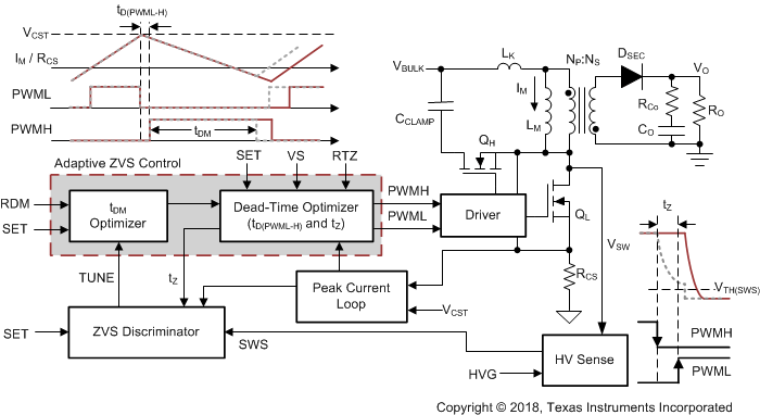
Figure 19 shows the simplified block diagram explaining the ZVS control of UCC28780. A high-voltage sensing network provides the replica of the switch node voltage waveform (VSW) with a limited “visible” voltage range that the SWS pin can handle. The ZVS discriminator identifies the ZVS condition and determines the adjustment direction for the on-time of PWMH (tDM) by detecting if VSW reaches a predetermined ZVS threshold, VTH(SWS), within tZ, where tZ is the targeted zero voltage transition time of VSW controlled by the PWMH-to-PWML dead-time optimizer.
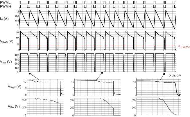
In Figure 19, VSW of the current switching cycle in the dashed line has not reached VTH(SWS) after tZ expires. The ZVS discriminator sends a TUNE signal to increase tDM for the next switching cycle in the solid line, such that the negative magnetizing current (IM-) can be increased to bring VSW down to a lower level in the same tZ. After a few switching cycles, the tDM optimizer settles and locks into ZVS operation of the low-side switch (QL). In steady-state, there is a fine adjustment on tDM, which is the least significant bit (LSB) of the ZVS tuning loop. This small change of tDM in each switching cycle is too small to significantly move the ZVS condition away from the desired operating point. Figure 20 demonstrates how fast the ZVS control can lock into ZVS operation. Before the ZVS loop is settled, UCC28780 starts in a valley-switching mode as tDM is not long enough to create sufficient IM-. Within 15 switching cycles, the ZVS tuning loop settles and begins toggling tDM with an LSB.
 Figure 19. Block Diagram of Adaptive ZVS Control
 Figure 20. Auto-Tuning Process of Adaptive ZVS Control