ZHCSH21A October 2017 – February 2018 UCC28780
PRODUCTION DATA.
- 1 特性
- 2 应用
- 3 说明
- 4 修订历史记录
- 5 Pin Configuration and Functions
- 6 Specifications
-
7 Detailed Description
- 7.1 Overview
- 7.2 Functional Block Diagram
- 7.3
Detailed Pin Description
- 7.3.1 BUR Pin (Programmable Burst Mode)
- 7.3.2 FB Pin (Feedback Pin)
- 7.3.3 VDD Pin (Device Bias Supply)
- 7.3.4 REF Pin (Internal 5-V Bias)
- 7.3.5 HVG and SWS Pins
- 7.3.6 RTZ Pin (Sets Delay for Transition Time to Zero)
- 7.3.7 RDM Pin (Sets Synthesized Demagnetization Time for ZVS Tuning)
- 7.3.8 RUN Pin (Driver Enable Pin)
- 7.3.9 SET Pin
- 7.4
Device Functional Modes
- 7.4.1 Adaptive ZVS Control with Auto-Tuning
- 7.4.2 Dead-Time Optimization
- 7.4.3 Control Law across Entire Load Range
- 7.4.4 Adaptive Amplitude Modulation (AAM)
- 7.4.5 Adaptive Burst Mode (ABM)
- 7.4.6 Low Power Mode (LPM)
- 7.4.7 Standby Power Mode (SBP)
- 7.4.8 Startup Sequence
- 7.4.9 Survival Mode of VDD
- 7.4.10 System Fault Protections
- 7.4.11 Pin Open/Short Protections
-
8 Application and Implementation
- 8.1 Application Information
- 8.2
Typical Application Circuit
- 8.2.1 Design Requirements
- 8.2.2 Detailed Design Procedure
- 8.2.3 Application Curves
- 9 Power Supply Recommendations
- 10Layout
- 11器件和文档支持
- 12机械、封装和可订购信息
封装选项
请参考 PDF 数据表获取器件具体的封装图。
机械数据 (封装 | 引脚)
- D|16
- RTE|16
散热焊盘机械数据 (封装 | 引脚)
- RTE|16
订购信息
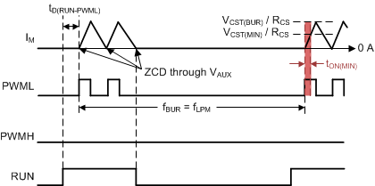
7.4.6 Low Power Mode (LPM)
As NSW drops to two in ABM and the condition of fBUR less than fBUR(LR) is qualified under two consecutive burst periods, UCC28780 enters into LPM mode and disables PWMH. The purpose of LPM is to provide a soft peak current transition between VCST(BUR) and VCST(MIN). LPM fixes NSW at two and sets fBUR equal to fLPM of 25 kHz. In LPM mode, VCST is controlled to regulate the output voltage. At the start of each burst packet, after RUN pulls high, tD(RUN-PWML) is used to wake up both the gate driver and UCC28780. With PWMH disabled, the two PWML pulses turn on QL close to valley-switching by sensing ZCD. When ZCD is detected again at the end of the second pulse, the RUN pin goes low and the UCC28780 enters its low-power wait state. In LPM mode, the minimum on-time of PWML can be further reduced to tON(MIN), to allow the peak magnetizing current to be reduced beyond the level limited by tCSLEB of the peak current loop. In this condition, operation of the LPM control loop is changed from a current-mode control to a voltage-mode control, so the on-time adjustment of PWML is not limited to tCSLEB. With this feature, before fBUR starts to fall below fLPM and enters the audible frequency range of SBP mode, the peak current is low enough to limit the magnitude of audible excitation.
 Figure 27. PWM Pattern in LPM