ZHCSH21A October   2017  – February 2018 UCC28780

PRODUCTION DATA.  

  1. 特性
  2. 应用
  3. 说明
    1.     Device Images
      1.      简化原理图
      2.      45W、20V GaN-ACF 适配器效率
  4. 修订历史记录
  5. Pin Configuration and Functions
    1.     Pin Functions
  6. Specifications
    1. 6.1 Absolute Maximum Ratings
    2. 6.2 ESD Ratings
    3. 6.3 Recommended Operating Conditions
    4. 6.4 Thermal Information of SOIC
    5. 6.5 Thermal Information of WQFN
    6. 6.6 Electrical Characteristics
    7. 6.7 Typical Characteristics
  7. Detailed Description
    1. 7.1 Overview
    2. 7.2 Functional Block Diagram
    3. 7.3 Detailed Pin Description
      1. 7.3.1 BUR Pin (Programmable Burst Mode)
      2. 7.3.2 FB Pin (Feedback Pin)
      3. 7.3.3 VDD Pin (Device Bias Supply)
      4. 7.3.4 REF Pin (Internal 5-V Bias)
      5. 7.3.5 HVG and SWS Pins
      6. 7.3.6 RTZ Pin (Sets Delay for Transition Time to Zero)
      7. 7.3.7 RDM Pin (Sets Synthesized Demagnetization Time for ZVS Tuning)
      8. 7.3.8 RUN Pin (Driver Enable Pin)
      9. 7.3.9 SET Pin
    4. 7.4 Device Functional Modes
      1. 7.4.1  Adaptive ZVS Control with Auto-Tuning
      2. 7.4.2  Dead-Time Optimization
      3. 7.4.3  Control Law across Entire Load Range
      4. 7.4.4  Adaptive Amplitude Modulation (AAM)
      5. 7.4.5  Adaptive Burst Mode (ABM)
      6. 7.4.6  Low Power Mode (LPM)
      7. 7.4.7  Standby Power Mode (SBP)
      8. 7.4.8  Startup Sequence
      9. 7.4.9  Survival Mode of VDD
      10. 7.4.10 System Fault Protections
        1. 7.4.10.1 Brown-In and Brown-Out
        2. 7.4.10.2 Output Over-Voltage Protection
        3. 7.4.10.3 Over-Temperature Protection
        4. 7.4.10.4 Programmable Over-Power Protection
        5. 7.4.10.5 Peak Current Limit
        6. 7.4.10.6 Output Short-Circuit Protection
        7. 7.4.10.7 Over-Current Protection
        8. 7.4.10.8 Thermal Shutdown
      11. 7.4.11 Pin Open/Short Protections
        1. 7.4.11.1 Protections on CS pin Fault
        2. 7.4.11.2 Protections on HVG pin Fault
        3. 7.4.11.3 Protections on RDM and RTZ pin Faults
  8. Application and Implementation
    1. 8.1 Application Information
    2. 8.2 Typical Application Circuit
      1. 8.2.1 Design Requirements
      2. 8.2.2 Detailed Design Procedure
        1. 8.2.2.1 Input Bulk Capacitance and Minimum Bulk Voltage
        2. 8.2.2.2 Transformer Calculations
          1. 8.2.2.2.1 Primary-to-Secondary Turns Ratio (NPS)
          2. 8.2.2.2.2 Primary Magnetizing Inductance (LM)
          3. 8.2.2.2.3 Primary Turns (NP)
          4. 8.2.2.2.4 Secondary Turns (NS)
          5. 8.2.2.2.5 Turns of Auxiliary Winding (NA)
          6. 8.2.2.2.6 Winding and Magnetic Core Materials
        3. 8.2.2.3 Clamp Capacitor Calculation
        4. 8.2.2.4 Bleed-Resistor Calculation
        5. 8.2.2.5 Output Filter Calculation
        6. 8.2.2.6 Calculation of ZVS Sensing Network
        7. 8.2.2.7 Calculation of Compensation Network
      3. 8.2.3 Application Curves
  9. Power Supply Recommendations
  10. 10Layout
    1. 10.1 Layout Guidelines
      1. 10.1.1 General Considerations
      2. 10.1.2 RDM and RTZ Pins
      3. 10.1.3 SWS Pin
      4. 10.1.4 VS Pin
      5. 10.1.5 BUR Pin
      6. 10.1.6 FB Pin
      7. 10.1.7 CS Pin
      8. 10.1.8 GND Pin
    2. 10.2 Layout Example
  11. 11器件和文档支持
    1. 11.1 文档支持
      1. 11.1.1 相关文档
    2. 11.2 接收文档更新通知
    3. 11.3 社区资源
    4. 11.4 商标
    5. 11.5 静电放电警告
    6. 11.6 Glossary
  12. 12机械、封装和可订购信息

封装选项

请参考 PDF 数据表获取器件具体的封装图。

机械数据 (封装 | 引脚)
  • D|16
  • RTE|16
散热焊盘机械数据 (封装 | 引脚)
订购信息

Standby Power Mode (SBP)

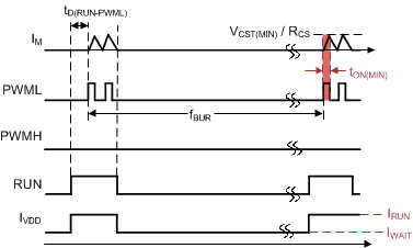
As VCST drops to VCST(MIN), UCC28780 enters into SBP mode and PWMH continues to stay disabled. The purpose of SBP is to lower fBUR in order to minimize standby power. SBP fixes NSW at two and VCST to VCST(MIN), while the burst off-time is adjusted to regulate the output voltage. As fBUR is well below fLPM, the switching-related loss can be minimized. In addition, lowering fBUR forces both the gate driver and UCC28780 to remain in wait states longer to minimize the static power loss. The equivalent static current of the UCC28780 in SBP can be represented as

Equation 12. UCC28780 Equ-iVDD(SBP).gif
UCC28780 PWM-pattern-in-SBP.gifFigure 28. PWM Pattern in SBP