ZHCSH21A October 2017 – February 2018 UCC28780
PRODUCTION DATA.
- 1 特性
- 2 应用
- 3 说明
- 4 修订历史记录
- 5 Pin Configuration and Functions
- 6 Specifications
-
7 Detailed Description
- 7.1 Overview
- 7.2 Functional Block Diagram
- 7.3
Detailed Pin Description
- 7.3.1 BUR Pin (Programmable Burst Mode)
- 7.3.2 FB Pin (Feedback Pin)
- 7.3.3 VDD Pin (Device Bias Supply)
- 7.3.4 REF Pin (Internal 5-V Bias)
- 7.3.5 HVG and SWS Pins
- 7.3.6 RTZ Pin (Sets Delay for Transition Time to Zero)
- 7.3.7 RDM Pin (Sets Synthesized Demagnetization Time for ZVS Tuning)
- 7.3.8 RUN Pin (Driver Enable Pin)
- 7.3.9 SET Pin
- 7.4
Device Functional Modes
- 7.4.1 Adaptive ZVS Control with Auto-Tuning
- 7.4.2 Dead-Time Optimization
- 7.4.3 Control Law across Entire Load Range
- 7.4.4 Adaptive Amplitude Modulation (AAM)
- 7.4.5 Adaptive Burst Mode (ABM)
- 7.4.6 Low Power Mode (LPM)
- 7.4.7 Standby Power Mode (SBP)
- 7.4.8 Startup Sequence
- 7.4.9 Survival Mode of VDD
- 7.4.10 System Fault Protections
- 7.4.11 Pin Open/Short Protections
-
8 Application and Implementation
- 8.1 Application Information
- 8.2
Typical Application Circuit
- 8.2.1 Design Requirements
- 8.2.2 Detailed Design Procedure
- 8.2.3 Application Curves
- 9 Power Supply Recommendations
- 10Layout
- 11器件和文档支持
- 12机械、封装和可订购信息
封装选项
请参考 PDF 数据表获取器件具体的封装图。
机械数据 (封装 | 引脚)
- D|16
- RTE|16
散热焊盘机械数据 (封装 | 引脚)
- RTE|16
订购信息
7.4.10.1 Brown-In and Brown-Out
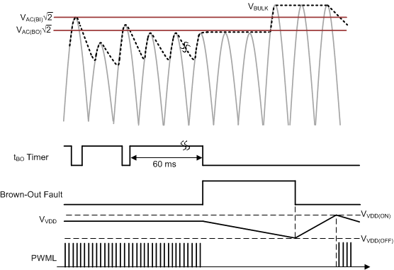
The VS pin senses the negative voltage level of the auxiliary winding during the on-time of low-side switch (QL) to detect an under-voltage condition of the input AC line. When the bulk voltage (VBULK) is too low, UCC28780 stops switching and no VO restart attempt is made until the AC input line voltage is back into normal range. As QL turns on with PWML, the negative voltage level of auxiliary winding voltage (VAUX) is equal to VBULK divided by primary-to-auxiliary turns ratio (NPA) of the transformer, which is NP / NA,. During this time, the voltage on VS pin is clamped to about 250 mV below GND. As a result, VAUX can create a line-sensing current (IVSL) out of the VS pin flowing through the upper resistor of the voltage divider on VS pin (RVS1). With IVSL proportional to VBULK, it can be used to compare against two under-voltage thresholds, IVSL(RUN) and IVSL(STOP).
The target brown-in AC voltage (VAC(BI)) can be programmed by the proper selection of RVS1. For every UVLO cycle of VDD, there are at least four initial test pulses from PWML to check IVSLcondition. IVSL of the first test pulse is ignored. If IVSL ≤ IVSL(RUN) is valid for the rest three consecutive test pulses, the controller stops switching, the RUN pin goes low, and a new UVLO start cycle is initiated after VVDD reaches VVDD(OFF). On the other hand, if IVSL> IVSL(RUN) occurs, VO soft start sequence is initiated.

The brown-out AC voltage (VAC(BO)) is set internally by around 83% of VAC(BI), which provides enough hysteresis to compensate for possible sensing errors through the auxiliary winding. A 60-ms timer (tBO) is used to bypass the effect of line ripple content on the IVSL sensing. Only when the IVSL ≤ IVSL(STOP) condition lasts longer than 60 ms, i.e. typically three line cycles of 50 Hz, the brown-out fault is triggered. The fault is reset after VVDD reaches VVDD(OFF). Figure 31 shows an example of the timing sequence of brown-in and brown-out protections.
.gif)
 Figure 31. Timing Diagram of Brown In/Out