ZHCSH21A October 2017 – February 2018 UCC28780
PRODUCTION DATA.
- 1 特性
- 2 应用
- 3 说明
- 4 修订历史记录
- 5 Pin Configuration and Functions
- 6 Specifications
-
7 Detailed Description
- 7.1 Overview
- 7.2 Functional Block Diagram
- 7.3
Detailed Pin Description
- 7.3.1 BUR Pin (Programmable Burst Mode)
- 7.3.2 FB Pin (Feedback Pin)
- 7.3.3 VDD Pin (Device Bias Supply)
- 7.3.4 REF Pin (Internal 5-V Bias)
- 7.3.5 HVG and SWS Pins
- 7.3.6 RTZ Pin (Sets Delay for Transition Time to Zero)
- 7.3.7 RDM Pin (Sets Synthesized Demagnetization Time for ZVS Tuning)
- 7.3.8 RUN Pin (Driver Enable Pin)
- 7.3.9 SET Pin
- 7.4
Device Functional Modes
- 7.4.1 Adaptive ZVS Control with Auto-Tuning
- 7.4.2 Dead-Time Optimization
- 7.4.3 Control Law across Entire Load Range
- 7.4.4 Adaptive Amplitude Modulation (AAM)
- 7.4.5 Adaptive Burst Mode (ABM)
- 7.4.6 Low Power Mode (LPM)
- 7.4.7 Standby Power Mode (SBP)
- 7.4.8 Startup Sequence
- 7.4.9 Survival Mode of VDD
- 7.4.10 System Fault Protections
- 7.4.11 Pin Open/Short Protections
-
8 Application and Implementation
- 8.1 Application Information
- 8.2
Typical Application Circuit
- 8.2.1 Design Requirements
- 8.2.2 Detailed Design Procedure
- 8.2.3 Application Curves
- 9 Power Supply Recommendations
- 10Layout
- 11器件和文档支持
- 12机械、封装和可订购信息
封装选项
请参考 PDF 数据表获取器件具体的封装图。
机械数据 (封装 | 引脚)
- D|16
- RTE|16
散热焊盘机械数据 (封装 | 引脚)
- RTE|16
订购信息
10.1.1 General Considerations
Designing for high power density requires to consider noise coupling and thermal management. A four-layer PCB structure is highly recommended to use inner layers to help reduce current loop areas and provide heat-spreading for surface-mount semiconductors.
- Provide internal-layer copper areas to improve heat dissipation of high-power SMDs, particularly for MOSFETs and power diodes.
- To avoid capacitive noise coupling, do not cross outer-layer signals over copper areas with high-frequency switching voltage.
- To avoid inductive noise coupling, keep switching current loops as small as possible, and do not run signal tracks in parallel with such loops.
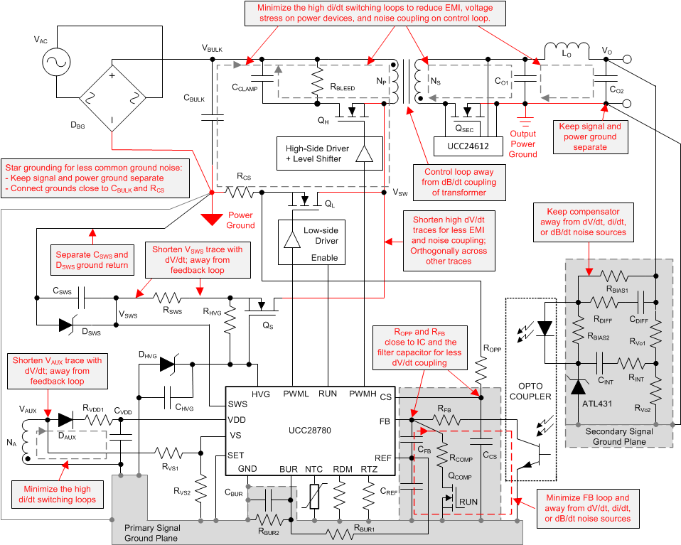
Figure 54 summarizes the critical layout guidelines, and more detail will be also be further elaborated in the descriptions below.
 Figure 54. Schematic with Layout Considerations